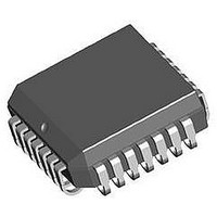
CS61574A-IL1Z Cirrus Logic Inc, CS61574A-IL1Z Datasheet - Page 23

CS61574A-IL1Z
Manufacturer Part Number
CS61574A-IL1Z
Description
IC T1/E1 Ln Intrfc Unit F/Stratum-4 Apps
Manufacturer
Cirrus Logic Inc
Datasheet
1.CDB61574A.pdf
(34 pages)
Specifications of CS61574A-IL1Z
Ic Interface Type
Serial
Supply Voltage Range
4.75V To 5.25V
Power Dissipation Pd
290mW
Operating Temperature Range
-40°C To +85°C
Digital Ic Case Style
LCC
No. Of Pins
28
Rohs Compliant
Yes
Lead Free Status / RoHS Status
Lead free / RoHS Compliant
Available stocks
Company
Part Number
Manufacturer
Quantity
Price
Company:
Part Number:
CS61574A-IL1Z
Manufacturer:
Cirrus Logic Inc
Quantity:
10 000
Company:
Part Number:
CS61574A-IL1ZR
Manufacturer:
CIRRUS
Quantity:
1 000
Company:
Part Number:
CS61574A-IL1ZR
Manufacturer:
Cirrus Logic Inc
Quantity:
10 000
Power Supplies
RGND - Ground, Pin 22.
RV+ - Power Supply, Pin 21.
TGND - Ground, Transmit Driver, Pin 14.
TV+ - Power Supply, Transmit Driver, Pin 15.
Oscillator
XTALIN, XTALOUT - Crystal Connections, Pins 9 and 10.
Control
ACLKI - Alternate External Clock Input, Pin 1.
CLKE - Clock Edge, Pin 28. (Host Mode)
CS - Chip Select, Pin 26. (Host Mode)
INT - Receive Alarm Interrupt, Pin 23. (Host Mode)
DS154F3
Power supply ground for all subcircuits except the transmit driver; typically 0 Volts.
Power supply for all subcircuits except the transmit driver; typically +5 Volts.
Power supply ground for the transmit driver; typically 0 Volts.
Power supply for the transmit driver; typically +5 Volts. TV+ must not exceed RV+ by more than
0.3 V.
A 6.176 MHz (or 8.192 MHz) crystal should be connected across these pins. If a 1.544 MHz (or
2.048 MHz) clock is provided on ACLKI (pin 1), the jitter attenuator may be disabled by tying
XTALIN, Pin 9 to RV+ through a 1 kΩ resistor, and floating XTALOUT, Pin 10.
Overdriving the oscillator with an external clock is not supported. See Appendix A.
A 1.544 MHz (or 2.048 MHz) clock may be input to ACLKI, or this pin must be tied to ground.
During LOS, the ACLKI input signal, if present, is output on RCLK through the jitter attenuator.
Setting CLKE to logic 1 causes RPOS and RNEG to be valid on the falling edge of RCLK, and
SDO to be valid on the rising edge of SCLK. Conversely, setting CLKE to logic 0 causes RPOS
and RNEG to be valid on the rising edge of RCLK, and SDO to be valid on the falling edge of
SCLK.
This pin must transition from high to low to read or write the serial port.
Goes low when LOS or DPM change state to flag the host processor. INT is cleared by writing
"clear LOS" or "clear DPM" to the register. INT is an open drain output and should be tied to the
power supply through a resistor.
CS61574A CS61575
23


