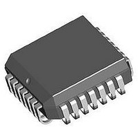
CS61574A-IL1Z Cirrus Logic Inc, CS61574A-IL1Z Datasheet - Page 25

CS61574A-IL1Z
Manufacturer Part Number
CS61574A-IL1Z
Description
IC T1/E1 Ln Intrfc Unit F/Stratum-4 Apps
Manufacturer
Cirrus Logic Inc
Datasheet
1.CDB61574A.pdf
(34 pages)
Specifications of CS61574A-IL1Z
Ic Interface Type
Serial
Supply Voltage Range
4.75V To 5.25V
Power Dissipation Pd
290mW
Operating Temperature Range
-40°C To +85°C
Digital Ic Case Style
LCC
No. Of Pins
28
Rohs Compliant
Yes
Lead Free Status / RoHS Status
Lead free / RoHS Compliant
Available stocks
Company
Part Number
Manufacturer
Quantity
Price
Company:
Part Number:
CS61574A-IL1Z
Manufacturer:
Cirrus Logic Inc
Quantity:
10 000
Company:
Part Number:
CS61574A-IL1ZR
Manufacturer:
CIRRUS
Quantity:
1 000
Company:
Part Number:
CS61574A-IL1ZR
Manufacturer:
Cirrus Logic Inc
Quantity:
10 000
TAOS - Transmit All Ones Select, Pin 28. (Hardware and Extended Hardware Modes)
TCODE - Transmitter Encoder Select, Pin 4. (Extended Hardware Mode)
Data
RCLK - Recovered Clock, Pin 8.
RDATA - Receive Data - Pin 7. (Extended Hardware Mode)
RPOS, RNEG - Receive Positive Data, Receive Negative Data, Pins 6 and 7. (Hardware and Host
Modes)
RTIP, RRING - Receive Tip, Receive Ring, Pins 19 and 20.
TCLK - Transmit Clock, Pin 2.
TDATA - Transmit Data, Pin 3. (Extended Hardware Mode)
TPOS, TNEG - Transmit Positive Data, Transmit Negative Data, Pins 3 and 4. (Hardware and
Host Modes)
DS154F3
Setting TAOS to a logic 1 causes continuous ones to be transmitted at the frequency determined
by TCLK.
Setting TCODE low enables B8ZS or HDB3 zero substitution in the transmitter encoder. Setting
TCODE high enables the AMI transmitter encoder .
The receiver recovered clock generated by the jitter attenuator is output on this pin.When in the
loss of signal state ACLKI (if present) is output on RCLK via the jitter attenuator. If ACLKI is
not present during LOS, RCLK is forced to the center frequency of the crystal oscillator..
Data recovered from the RTIP and RRING inputs is output at this pin, after being decoded by the
line code decoder. RDATA is NRZ. RDATA is stable and valid on the falling edge of RCLK.
The receiver recovered NRZ digital data is output on these pins. In the Hardware Mode, RPOS
and RNEG are stable and valid on the rising edge of RCLK. In the Host Mode, CLKE determines
the clock edge for which RPOS and RNEG are stable and valid. See Table 5. A positive pulse
(with respect to ground) received on the RTIP pin generates a logic 1 on RPOS, and a positive
pulse received on the RRING pin generates a logic 1 on RNEG.
The AMI receive signal is input to these pins. A center-tapped, center-grounded, 2:1, step-up
transformer is required on these inputs, as shown in Figure A1 in the Applications section. Data
and clock are recovered and output on RCLK and RPOS/RNEG or RDATA.
The1.544 MHz (or 2.048 MHz) transmit clock is input on this pin. TPOS/TNEG or TDATA are
sampled on the falling edge of TCLK.
Transmitter NRZ input data which passes through the line code encoder, and is then driven on to
the line through TTIP and TRING. TDATA is sampled on the falling edge of TCLK.
Inputs for clock and data to be transmitted. The signal is driven on to the line through TTIP and
TRING. TPOS and TNEG are sampled on the falling edge of TCLK. A TPOS input causes a
positive pulse to be transmitted, while a TNEG input causes a negative pulse to be transmitted.
CS61574A CS61575
25


