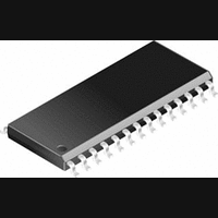
CS8405A-CS Cirrus Logic Inc, CS8405A-CS Datasheet - Page 24

CS8405A-CS
Manufacturer Part Number
CS8405A-CS
Description
Transceiver IC
Manufacturer
Cirrus Logic Inc
Datasheet
1.CS8405A-CS.pdf
(36 pages)
Specifications of CS8405A-CS
Peak Reflow Compatible (260 C)
No
Supply Voltage
5V
Supply Voltage Max
5V
Transceiver Type
Digital Audio
Leaded Process Compatible
No
Mounting Type
Surface Mount
Interface Type
Serial
Package / Case
28-SOIC
Lead Free Status / RoHS Status
Contains lead / RoHS non-compliant
Available stocks
Company
Part Number
Manufacturer
Quantity
Price
Company:
Part Number:
CS8405A-CS
Manufacturer:
SILICOM
Quantity:
89
Part Number:
CS8405A-CS
Manufacturer:
CIRRUS
Quantity:
20 000
Part Number:
CS8405A-CSEP
Manufacturer:
CIRRUS
Quantity:
20 000
Part Number:
CS8405A-CSZ
Manufacturer:
CIRRUS
Quantity:
20 000
9. PIN DESCRIPTION - SOFTWARE MODE
24
SDA/CDOUT
AD0/CS
AD2
RXP
DGND2
DGND4
DGND3
DGND
VD+
VL+
RST
NC1
NC2
NC3
NC4
NC5
ILRCK
ISCLK
SDIN
TCBL
22
23
10
11
16
17
18
12
13
14
15
1
2
3
4
5
7
8
6
9
Serial Control Data I/O (Two-Wire Mode) / Data Out (SPI) (Input/Output) - In Two-Wire Mode, SDA is
the control I/O data line. SDA is open drain and requires an external pull-up resistor to VL+. In SPI
mode, CDOUT is the output data from the control port interface on the CS8405A
Address Bit 0 (Two-Wire Mode) / Control Port Chip Select (SPI) (Input/Output) - A falling edge on
this pin puts the CS8405A into SPI control port mode. With no falling edge, the CS8405A defaults to
Two-Wire mode. In Two-Wire mode, AD0 is a chip address pin. In SPI mode, CS is used to enable the
control port interface on the CS8405A
Address Bit 2 (Two-Wire Mode) (Input) - Determines the AD2 address bit for the control port in Two-
Wire mode, and should be connected to DGND or VL+. If SPI mode is used, the AD2 pin should be con-
nected to DGND.
Auxiliary AES3 Receiver Port (Input) - Input for an alternate, already AES3 coded, audio data
Digital Ground (Input) - Ground for the digital section.
Positive Digital Power (Input) - Typically +5 V. VD+ must be +5 V while VL+ may be operated at 3.3 V
Reset (Input) - When RST is low, the CS8405A enters a low power mode and all internal states are
reset. On initial power up, RST must be held low until the power supply is stable, and all input clocks are
stable in frequency and phase. This is particularly true in hardware mode with multiple CS8405A
devices, where synchronization between devices is important.
No Connect - These pins should not be connected to any signals or PCB trace. They may be driven
high and/or low by the CS8405A.
Serial Audio Input Left/Right Clock (Input/Output) - Word rate clock for the audio data on the SDIN
pin.
Serial Audio Bit Clock (Input/Output) - Serial bit clock for audio data on the SDIN pin.
Serial Audio Data Port (Input) - Audio data serial input pin.
Transmit Channel Status Block Start (Input/Output) - When operated as output, TCBL is high during
the first sub-frame of a transmitted channel status block, and low at all other times. When operated as
input, driving TCBL high for at least three OMCK clocks will cause the next transmitted sub-frame to be
the start of a channel status block.
CS8405A
DS469PP4
source.


