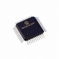
PIC16LC774-I/PQ Microchip Technology, PIC16LC774-I/PQ Datasheet - Page 114

PIC16LC774-I/PQ
Manufacturer Part Number
PIC16LC774-I/PQ
Description
44 PIN, 7KB OTP, 256 RAM, 33 I/O,
Manufacturer
Microchip Technology
Series
PIC® 16Cr
Specifications of PIC16LC774-I/PQ
Rohs Compliant
YES
Core Processor
PIC
Core Size
8-Bit
Speed
20MHz
Connectivity
I²C, SPI, UART/USART
Peripherals
Brown-out Detect/Reset, POR, PWM, WDT
Number Of I /o
33
Program Memory Size
7KB (4K x 14)
Program Memory Type
OTP
Ram Size
256 x 8
Voltage - Supply (vcc/vdd)
2.5 V ~ 5.5 V
Data Converters
A/D 10x12b
Oscillator Type
External
Operating Temperature
-40°C ~ 85°C
Package / Case
44-MQFP, 44-PQFP
Processor Series
PIC16LC
Core
PIC
Data Bus Width
8 bit
Data Ram Size
256 B
Interface Type
I2C, SPI, SSP, UART
Maximum Clock Frequency
20 MHz
Number Of Programmable I/os
33
Number Of Timers
3 bit
Operating Supply Voltage
2.5 V to 5.5 V
Maximum Operating Temperature
+ 85 C
Mounting Style
SMD/SMT
3rd Party Development Tools
52715-96, 52716-328, 52717-734
Development Tools By Supplier
ICE2000, DM163022
Minimum Operating Temperature
- 40 C
On-chip Adc
10 bit
Lead Free Status / RoHS Status
Lead free / RoHS Compliant
Eeprom Size
-
Lead Free Status / Rohs Status
Details
Available stocks
Company
Part Number
Manufacturer
Quantity
Price
Company:
Part Number:
PIC16LC774-I/PQ
Manufacturer:
Microchip Technology
Quantity:
10 000
PIC16C77X
FIGURE 10-2: REFCON: VOLTAGE REFERENCE CONTROL REGISTER
10.1
The bandgap module generates a stable voltage refer-
ence of 1.22V over a range of temperatures and device
supply voltages. This module is enabled anytime any of
the following are enabled:
• Brown-out Reset
• Low-voltage Detect
• Either of the internal analog references (VRH,
Whenever the above are all disabled, the bandgap
module is disabled and draws no current.
10.2
The bandgap output voltage is used to generate two
stable references for the A/D converter module. These
references are enabled in software to provide the user
with the means to turn them on and off in order to min-
imize current consumption. Each reference can be indi-
vidually enabled.
The 4.096V reference (VRH) is enabled with control bit
VRHEN (REFCON<7>). When this bit is set, the gain
amplifier is enabled. After a specified start-up time a
stable reference of 4.096V is generated and can be
used by the A/D converter as the VRH input.
The 2.048V reference (VRL) is enabled by setting con-
trol bit VRLEN (REFCON<6>). When this bit is set, the
gain amplifier is enabled. After a specified start up time
a stable reference of 2.048V is generated and can be
used by the A/D converter as the VRL input.
DS30275A-page 114
VRL)
bit7
bit 7:
bit 6:
bit 5:
bit 4:
bit 3-0: Unimplemented: Read as '0’
VRHEN
R/W-0
Bandgap Voltage Reference
Internal V
VRHEN: Voltage Reference High Enable bit (VRH = 4.096V)
1 = Enabled, powers up reference generator
0 = Disabled, powers down reference generator if unused by LVD, BOR, or VRL
VRLEN: Voltage Reference Low Enable bit (VRL = 2.048V)
1 = Enabled, powers up reference generator
0 = Disabled, powers down reference generator if unused by LVD, BOR, or VRH
VRHOEN: High Voltage Reference Output Enable bit
1 = Enabled, VRH analog reference is presented on RA3 if enabled (VRHEN = 1)
0 = Disabled, analog reference is used internally only
VRLOEN: Low Voltage Reference Output Enable bit
1 = Enabled, VRL analog reference is presented on RA2 if enabled (VRLEN = 1)
0 = Disabled, analog reference is used internally only
VRLEN
R/W-0
REF
for A/D Converter
VRHOEN
R/W-0
VRLOEN
R/W-0
Advance Information
U-0
—
U-0
Each voltage reference can source/sink up to 5 mA of
current.
Each reference, if enabled, can be presented on an
external pin by setting the VRHOEN (high reference
output enable) or VRLOEN (low reference output
enable) control bit. If the reference is not enabled, the
VRHOEN and VRLOEN bits will have no effect on the
corresponding pin. The device specific pin can then be
used as general purpose I/O.
—
Note:
U-0
—
If VRH or VRL is enabled and the other ref-
erence (VRL or VRH), the BOR, and the
LVD modules are not enabled, the band-
gap will require a start-up time of no more
than 50 s before the bandgap reference is
stable. Before using the internal VRH or
VRL reference, ensure that the bandgap
reference voltage is stable by monitoring
the BGST bit in the LVDCON register. The
voltage references will not be reliable until
the bandgap is stable as shown by BGST
being set.
U-0
bit0
—
1999 Microchip Technology Inc.
R = Readable bit
W = Writable bit
U = Unimplemented
- n =Value at POR
bit, read as ‘0’
reset


