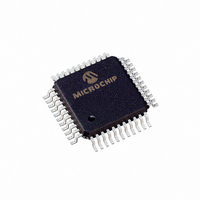
PIC16LC774-I/PQ Microchip Technology, PIC16LC774-I/PQ Datasheet - Page 30

PIC16LC774-I/PQ
Manufacturer Part Number
PIC16LC774-I/PQ
Description
44 PIN, 7KB OTP, 256 RAM, 33 I/O,
Manufacturer
Microchip Technology
Series
PIC® 16Cr
Specifications of PIC16LC774-I/PQ
Rohs Compliant
YES
Core Processor
PIC
Core Size
8-Bit
Speed
20MHz
Connectivity
I²C, SPI, UART/USART
Peripherals
Brown-out Detect/Reset, POR, PWM, WDT
Number Of I /o
33
Program Memory Size
7KB (4K x 14)
Program Memory Type
OTP
Ram Size
256 x 8
Voltage - Supply (vcc/vdd)
2.5 V ~ 5.5 V
Data Converters
A/D 10x12b
Oscillator Type
External
Operating Temperature
-40°C ~ 85°C
Package / Case
44-MQFP, 44-PQFP
Processor Series
PIC16LC
Core
PIC
Data Bus Width
8 bit
Data Ram Size
256 B
Interface Type
I2C, SPI, SSP, UART
Maximum Clock Frequency
20 MHz
Number Of Programmable I/os
33
Number Of Timers
3 bit
Operating Supply Voltage
2.5 V to 5.5 V
Maximum Operating Temperature
+ 85 C
Mounting Style
SMD/SMT
3rd Party Development Tools
52715-96, 52716-328, 52717-734
Development Tools By Supplier
ICE2000, DM163022
Minimum Operating Temperature
- 40 C
On-chip Adc
10 bit
Lead Free Status / RoHS Status
Lead free / RoHS Compliant
Eeprom Size
-
Lead Free Status / Rohs Status
Details
Available stocks
Company
Part Number
Manufacturer
Quantity
Price
Company:
Part Number:
PIC16LC774-I/PQ
Manufacturer:
Microchip Technology
Quantity:
10 000
- Current page: 30 of 201
- Download datasheet (3Mb)
PIC16C77X
The RB3 pin is multiplexed with analog channel 9 and
the low voltage detect input (RB3/AN9/LVDIN)
FIGURE 3-7:
DS30275A-page 30
Data bus
WR TRIS
WR Port
To A/D converter and LVD reference input
RBPU
Note 1: I/O pins have diode protection to V
(2)
2: To enable weak pull-ups, set the appropriate TRIS bit(s)
and clear the RBPU bit (OPTION_REG<7>).
RD TRIS
Data Latch
TRIS Latch
D
D
CK
CK
BLOCK DIAGRAM OF
RB3/AN9/LVDIN PIN
RD Port
Q
Q
Q
Analog
input mode
or LVD input
mode
EN
D
DD
and V
TTL
Input
Buffer
RD Port
SS
Advance Information
.
V
P
DD
weak
pull-up
I/O
pin
(1)
Four of PORTB’s pins, RB7:RB4, have an interrupt on
change feature. Only pins configured as inputs can
cause this interrupt to occur (i.e. any RB7:RB4 pin con-
figured as an output is excluded from the interrupt on
change comparison). The input pins (of RB7:RB4) are
compared with the old value latched on the last read of
PORTB. The “mismatch” outputs of RB7:RB4 are
OR’ed together to generate the RB Port Change Inter-
rupt with flag bit RBIF (INTCON<0>).
This interrupt can wake the device from SLEEP. The
user, in the interrupt service routine, can clear the inter-
rupt in the following manner:
a)
b)
A mismatch condition will continue to set flag bit RBIF.
Reading PORTB will end the mismatch condition, and
allow flag bit RBIF to be cleared.
The interrupt on change feature is recommended for
wake-up on key depression operation and operations
where PORTB is only used for the interrupt on change
feature. Polling of PORTB is not recommended while
using the interrupt on change feature.
FIGURE 3-8:
Data bus
WR TRIS
WR Port
RBPU
Note 1: I/O pins have diode protection to V
RB7:RB6 in serial programming mode
Set RBIF
From other
RB7:RB4 pins
Any read or write of PORTB. This will end the
mismatch condition.
Clear flag bit RBIF.
2: To enable weak pull-ups, set the appropriate TRIS bit(s)
(2)
and clear the RBPU bit (OPTION_REG<7>).
RD TRIS
RD Port
Data Latch
TRIS Latch
BLOCK DIAGRAM OF
RB7:RB4 PINS
D
D
CK
CK
Q
Q
1999 Microchip Technology Inc.
Q
Q
Latch
DD
EN
EN
D
D
and V
TTL
Input
Buffer
SS
V
P
DD
.
weak
pull-up
RD Port
Buffer
I/O
pin
Q1
Q3
(1)
ST
Related parts for PIC16LC774-I/PQ
Image
Part Number
Description
Manufacturer
Datasheet
Request
R

Part Number:
Description:
IC MCU OTP 8KX14 A/D PWM 40DIP
Manufacturer:
Microchip Technology
Datasheet:

Part Number:
Description:
IC MCU OTP 8KX14 A/D PWM 44-MQFP
Manufacturer:
Microchip Technology
Datasheet:

Part Number:
Description:
44 PIN, 14KB OTP, 368 RAM, 33 I/O,
Manufacturer:
Microchip Technology
Datasheet:

Part Number:
Description:
IC MCU OTP 8KX14 A/D PWM 44PLCC
Manufacturer:
Microchip Technology
Datasheet:

Part Number:
Description:
IC MCU OTP 8KX14 A/D PWM 44PLCC
Manufacturer:
Microchip Technology
Datasheet:

Part Number:
Description:
IC MCU OTP 8KX14 A/D PWM 40DIP
Manufacturer:
Microchip Technology
Datasheet:

Part Number:
Description:
IC MCU OTP 8KX14 A/D PWM 44-MQFP
Manufacturer:
Microchip Technology
Datasheet:

Part Number:
Description:
IC MCU OTP 8KX14 A/D PWM 44TQFP
Manufacturer:
Microchip Technology
Datasheet:

Part Number:
Description:
Manufacturer:
Microchip Technology Inc.
Datasheet:

Part Number:
Description:
Manufacturer:
Microchip Technology Inc.
Datasheet:

Part Number:
Description:
Manufacturer:
Microchip Technology Inc.
Datasheet:

Part Number:
Description:
Manufacturer:
Microchip Technology Inc.
Datasheet:


