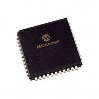
PIC17C42A-16/L Microchip Technology, PIC17C42A-16/L Datasheet - Page 233

PIC17C42A-16/L
Manufacturer Part Number
PIC17C42A-16/L
Description
IC,MICROCONTROLLER,8-BIT,PIC CPU,CMOS,LDCC,44PIN,PLASTIC
Manufacturer
Microchip Technology
Series
PIC® 17Cr
Datasheets
1.PIC16F616T-ISL.pdf
(8 pages)
2.PIC17C42A-16P.pdf
(241 pages)
3.PIC17C42A-16P.pdf
(4 pages)
Specifications of PIC17C42A-16/L
Rohs Compliant
YES
Core Processor
PIC
Core Size
8-Bit
Speed
16MHz
Connectivity
UART/USART
Peripherals
POR, PWM, WDT
Number Of I /o
33
Program Memory Size
4KB (2K x 16)
Program Memory Type
OTP
Ram Size
232 x 8
Voltage - Supply (vcc/vdd)
4.5 V ~ 6 V
Oscillator Type
External
Operating Temperature
0°C ~ 70°C
Package / Case
44-PLCC
Processor Series
PIC17C
Core
PIC
Data Bus Width
8 bit
Data Ram Size
232 B
Interface Type
SCI, USART
Maximum Clock Frequency
16 MHz
Number Of Programmable I/os
33
Number Of Timers
4
Maximum Operating Temperature
+ 70 C
Mounting Style
SMD/SMT
Development Tools By Supplier
ICE2000
Minimum Operating Temperature
0 C
Lead Free Status / RoHS Status
Lead free / RoHS Compliant
For Use With
AC164317 - MODULE SKT MPLAB PM3 44PLCCDVA17XL441 - DEVICE ADAPTER FOR PIC17C42A309-1007 - ADAPTER 44-PLCC ZIF TO 40-DIPAC174002 - MODULE SKT PROMATEII 44PLCC
Eeprom Size
-
Data Converters
-
Lead Free Status / Rohs Status
Details
Other names
PIC17C42A-16/LR
PIC17C42A-16/LR
PIC17C42A-16/LR
Available stocks
Company
Part Number
Manufacturer
Quantity
Price
Company:
Part Number:
PIC17C42A-16/L
Manufacturer:
Microchip Technology
Quantity:
10 000
Figure 19-2:
Figure 19-3:
Figure 19-4:
Figure 19-5:
Figure 19-6:
Figure 19-7:
Figure 19-8:
Figure 19-9:
Figure 19-10: USART Module: Synchronous
Figure 19-11: Memory Interface Write Timing
Figure 19-12: Memory Interface Read Timing
Figure 20-1:
Figure 20-2:
Figure 20-3:
Figure 20-4:
Figure 20-5:
Figure 20-6:
Figure 20-7:
Figure 20-8:
Figure 20-9:
Figure 20-10: Maximum I
Figure 20-11: Typical I
Figure 20-12: Maximum I
Figure 20-13: WDT Timer Time-Out Period vs. V
Figure 20-14: I
Figure 20-15: I
Figure 20-16: I
Figure 20-17: I
Figure 20-18: V
Figure 20-19: V
Figure 20-20: V
LIST OF TABLES
Table 1-1:
Table 3-1:
Table 4-1:
Table 4-2:
Table 4-3:
Table 4-4:
Table 5-1:
Table 6-1:
1996 Microchip Technology Inc.
External Clock Timing............................... 184
CLKOUT and I/O Timing........................... 185
Reset, Watchdog Timer,
Oscillator Start-Up Timer, and
Power-Up Timer Timing............................ 186
Timer0 Clock Timings ............................... 187
Timer1, Timer2, and Timer3 Clock
Timings ..................................................... 187
Capture Timings ....................................... 188
PWM Timings ........................................... 188
USART Module: Synchronous
Transmission (Master/Slave) Timing ........ 189
Receive (Master/Slave) Timing................. 189
(Not Supported in PIC17LC4X Devices)... 190
(Not Supported in PIC17LC4X Devices)... 191
Typical RC Oscillator Frequency vs.
Temperature ............................................. 193
Typical RC Oscillator Frequency
vs. V
Typical RC Oscillator Frequency
vs. V
Typical RC Oscillator Frequency
vs. V
Transconductance (gm) of LF Oscillator
vs. V
Transconductance (gm) of XT Oscillator
vs. V
Typical I
Clock 25 C)............................................... 197
Maximum I
Clock 125 C to -40 C) .............................. 197
Typical I
Disabled 25 C........................................... 198
Disabled.................................................... 198
Enabled 25 C............................................ 199
Enabled..................................................... 199
I/O Pins (TTL)
VS
Input (In XT and LF Modes) vs. V
PIC17CXX Family of Devices ....................... 6
Pinout Descriptions..................................... 12
Time-Out in Various Situations ................... 16
STATUS Bits and Their Significance .......... 16
Reset Condition for the Program Counter
and the CPUSTA Register.......................... 16
Initialization Conditions For Special
Function Registers...................................... 19
Interrupt Vectors/Priorities .......................... 25
Mode Memory Access ................................ 30
OH
OH
OL
OL
TH
TH
TH
. V
vs. V
vs. V
, V
vs. V
vs. V
(Input Threshold Voltage) of
(Input Threshold Voltage) of OSC1
DD
DD
DD
DD
DD
DD
IL
...................................................... 194
...................................................... 194
...................................................... 195
...................................................... 196
...................................................... 196
..................................................... 203
DD
PD
PD
OL
OL
of I/O Pins (Schmitt Trigger)
OH
OH
DD
PD
PD
, V
, V
vs. Frequency (External
vs. V
vs. V
, V
, V
DD
DD
vs. V
vs. V
vs. Frequency (External
DD
DD
VS
DD
DD
= 3V ............................... 201
= 5V ............................... 202
. V
= 3V .............................. 200
= 5V .............................. 201
DD
DD
Watchdog
Watchdog
DD
Watchdog
Watchdog
.............................. 202
DD
DD
........ 203
....... 200
Table 6-2:
Table 6-3:
Table 7-1:
Table 8-1:
Table 9-1:
Table 9-2:
Table 9-3:
Table 9-4:
Table 9-5:
Table 9-6:
Table 9-7:
Table 9-8:
Table 9-9:
Table 9-10:
Table 11-1:
Table 12-1:
Table 12-2:
Table 12-3:
Table 12-4:
Table 12-5:
Table 12-6:
Table 13-1:
Table 13-2:
Table 13-3:
Table 13-4:
Table 13-5:
Table 13-6:
Table 13-7:
Table 13-8:
Table 13-9:
Table 13-10:
Table 14-1:
Table 14-2:
Table 14-3:
Table 14-4:
Table 15-1:
Table 15-2:
Table 16-1:
Table 17-1:
Table 17-2:
Table 17-3:
Table 17-4:
Table 17-5:
Table 17-6:
Table 17-7:
Table 17-8:
EPROM Memory Access Time
Ordering Suffix ............................................31
Special Function Registers..........................34
Interrupt - Table Write Interaction................45
Performance Comparison ...........................49
PORTA Functions .......................................54
Registers/Bits Associated with PORTA.......54
PORTB Functions .......................................57
Registers/Bits Associated with PORTB.......57
PORTC Functions .......................................59
Registers/Bits Associated with PORTC.......59
PORTD Functions .......................................61
Registers/Bits Associated with PORTD.......61
PORTE Functions .......................................63
Registers/Bits Associated with PORTE.......63
Registers/Bits Associated with Timer0 ........70
Turning On 16-bit Timer ..............................74
Summary of Timer1 and Timer2
Registers .....................................................74
PWM Frequency vs. Resolution at
25 MHz ........................................................76
Registers/Bits Associated with PWM ..........77
Registers Associated with Capture .............79
Summary of TMR1, TMR2, and TMR3
Registers .....................................................81
Baud Rate Formula .....................................86
Registers Associated with Baud Rate
Generator ....................................................86
Baud Rates for Synchronous Mode ............87
Baud Rates for Asynchronous Mode...........88
Registers Associated with Asynchronous
Transmission ...............................................90
Registers Associated with Asynchronous
Reception ....................................................92
Registers Associated with Synchronous
Master Transmission ...................................94
Registers Associated with Synchronous
Master Reception ........................................96
Registers Associated with Synchronous
Slave Transmission .....................................98
Registers Associated with Synchronous
Slave Reception ..........................................98
Configuration Locations.............................100
Capacitor Selection for Ceramic
Resonators ................................................101
Capacitor Selection for Crystal
OscillatoR ..................................................101
Registers/Bits Associated with the
Watchdog Timer ........................................104
Opcode Field Descriptions ........................107
PIC17CXX Instruction Set .........................110
development tools from microchip.............146
Cross Reference of Device Specs for
Oscillator Configurations and Frequencies
of Operation (Commercial Devices) ..........148
External Clock Timing Requirements ........155
CLKOUT and I/O Timing Requirements....156
Reset, Watchdog Timer,
Oscillator Start-Up Timer and
Power-Up Timer Requirements.................157
Timer0 Clock Requirements......................158
Timer1, Timer2, and Timer3 Clock
Requirements ............................................158
Capture Requirements ..............................159
PWM Requirements ..................................159
PIC17C4X
DS30412C-page 233


