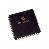
PIC17C42A-16/L Microchip Technology, PIC17C42A-16/L Datasheet - Page 91

PIC17C42A-16/L
Manufacturer Part Number
PIC17C42A-16/L
Description
IC,MICROCONTROLLER,8-BIT,PIC CPU,CMOS,LDCC,44PIN,PLASTIC
Manufacturer
Microchip Technology
Series
PIC® 17Cr
Datasheets
1.PIC16F616T-ISL.pdf
(8 pages)
2.PIC17C42A-16P.pdf
(241 pages)
3.PIC17C42A-16P.pdf
(4 pages)
Specifications of PIC17C42A-16/L
Rohs Compliant
YES
Core Processor
PIC
Core Size
8-Bit
Speed
16MHz
Connectivity
UART/USART
Peripherals
POR, PWM, WDT
Number Of I /o
33
Program Memory Size
4KB (2K x 16)
Program Memory Type
OTP
Ram Size
232 x 8
Voltage - Supply (vcc/vdd)
4.5 V ~ 6 V
Oscillator Type
External
Operating Temperature
0°C ~ 70°C
Package / Case
44-PLCC
Processor Series
PIC17C
Core
PIC
Data Bus Width
8 bit
Data Ram Size
232 B
Interface Type
SCI, USART
Maximum Clock Frequency
16 MHz
Number Of Programmable I/os
33
Number Of Timers
4
Maximum Operating Temperature
+ 70 C
Mounting Style
SMD/SMT
Development Tools By Supplier
ICE2000
Minimum Operating Temperature
0 C
Lead Free Status / RoHS Status
Lead free / RoHS Compliant
For Use With
AC164317 - MODULE SKT MPLAB PM3 44PLCCDVA17XL441 - DEVICE ADAPTER FOR PIC17C42A309-1007 - ADAPTER 44-PLCC ZIF TO 40-DIPAC174002 - MODULE SKT PROMATEII 44PLCC
Eeprom Size
-
Data Converters
-
Lead Free Status / Rohs Status
Details
Other names
PIC17C42A-16/LR
PIC17C42A-16/LR
PIC17C42A-16/LR
Available stocks
Company
Part Number
Manufacturer
Quantity
Price
Company:
Part Number:
PIC17C42A-16/L
Manufacturer:
Microchip Technology
Quantity:
10 000
- Current page: 91 of 241
- Download datasheet (2Mb)
13.2.2
The receiver block diagram is shown in Figure 13-4.
The data comes in the RA4/RX/DT pin and drives the
data recovery block. The data recovery block is actually
a high speed shifter operating at 16 times the baud
rate, whereas the main receive serial shifter operates
at the bit rate or at F
Once asynchronous mode is selected, reception is
enabled by setting bit CREN (RCSTA<4>).
The heart of the receiver is the receive (serial) shift reg-
ister (RSR). After sampling the stop bit, the received
data in the RSR is transferred to the RCREG (if it is
empty). If the transfer is complete, the interrupt bit
RCIF (PIR<0>) is set. The actual interrupt can be
enabled/disabled
(PIE<0>) bit. RCIF is a read only bit which is cleared by
the hardware. It is cleared when RCREG has been
read and is empty. RCREG is a double buffered regis-
ter; (i.e. it is a two deep FIFO). It is possible for two
bytes of data to be received and transferred to the
RCREG FIFO and a third byte begin shifting to the
RSR. On detection of the stop bit of the third byte, if the
RCREG is still full, then the overrun error bit,
OERR (RCSTA<1>) will be set. The word in the RSR
will be lost. RCREG can be read twice to retrieve the
two bytes in the FIFO. The OERR bit has to be cleared
in software which is done by resetting the receive logic
(CREN is set). If the OERR bit is set, transfers from the
RSR to RCREG are inhibited, so it is essential to clear
the OERR bit if it is set. The framing error bit
FERR (RCSTA<2>) is set if a stop bit is not detected.
FIGURE 13-7: RX PIN SAMPLING SCHEME
(RA4/RX/DT pin)
1996 Microchip Technology Inc.
baud CLK
USART ASYNCHRONOUS RECEIVER
x16 CLK
RX
by
OSC
1
.
setting/clearing
2
3
4
5
the
6
RCIE
7
Samples
8
9
Start bit
13.2.3
The data on the RA4/RX/DT pin is sampled three times
by a majority detect circuit to determine if a high or a
low level is present at the RA4/RX/DT pin. The sam-
pling is done on the seventh, eighth and ninth falling
edges of a x16 clock (Figure 11-3).
The x16 clock is a free running clock, and the three
sample points occur at a frequency of every 16 falling
edges.
10
Note:
11
SAMPLING
Baud CLK for all but start bit
12
The FERR and the 9th receive bit are buff-
ered the same way as the receive data.
Reading the RCREG register will allow the
RX9D and FERR bits to be loaded with val-
ues for the next received Received data;
therefore, it is essential for the user to read
the
RCREG in order not to lose the old FERR
and RX9D information.
13
RCSTA
14
15
register
PIC17C4X
16
1
DS30412C-page 91
before
2
Bit0
3
reading
Related parts for PIC17C42A-16/L
Image
Part Number
Description
Manufacturer
Datasheet
Request
R

Part Number:
Description:
IC MCU OTP 2KX16 PWM 40DIP
Manufacturer:
Microchip Technology
Datasheet:

Part Number:
Description:
IC MCU OTP 2KX16 PWM 40DIP
Manufacturer:
Microchip Technology
Datasheet:

Part Number:
Description:
IC MCU OTP 2KX16 PWM 44-MQFP
Manufacturer:
Microchip Technology
Datasheet:

Part Number:
Description:
IC MCU OTP 2KX16 PWM 44PLCC
Manufacturer:
Microchip Technology
Datasheet:

Part Number:
Description:
IC MCU OTP 2KX16 PWM 44PLCC
Manufacturer:
Microchip Technology
Datasheet:

Part Number:
Description:
IC MCU OTP 2KX16 PWM 44-MQFP
Manufacturer:
Microchip Technology
Datasheet:

Part Number:
Description:
IC MCU OTP 2KX16 PWM 44TQFP
Manufacturer:
Microchip Technology
Datasheet:

Part Number:
Description:
IC MCU OTP 2KX16 PWM 44-MQFP
Manufacturer:
Microchip Technology
Datasheet:

Part Number:
Description:
IC MCU OTP 2KX16 PWM 44TQFP
Manufacturer:
Microchip Technology
Datasheet:

Part Number:
Description:
IC MCU OTP 2KX16 PWM 40DIP
Manufacturer:
Microchip Technology
Datasheet:

Part Number:
Description:
IC MCU OTP 2KX16 PWM 40DIP
Manufacturer:
Microchip Technology
Datasheet:

Part Number:
Description:
IC MCU OTP 2KX16 PWM 40DIP
Manufacturer:
Microchip Technology
Datasheet:

Part Number:
Description:
IC MCU OTP 2KX16 PWM 44-MQFP
Manufacturer:
Microchip Technology
Datasheet:

Part Number:
Description:
IC MCU OTP 2KX16 PWM 44PLCC
Manufacturer:
Microchip Technology
Datasheet:

Part Number:
Description:
IC MCU OTP 2KX16 PWM 44-MQFP
Manufacturer:
Microchip Technology
Datasheet:


