PIC18C601-I/L Microchip Technology, PIC18C601-I/L Datasheet - Page 39
PIC18C601-I/L
Manufacturer Part Number
PIC18C601-I/L
Description
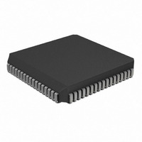
IC,MICROCONTROLLER,8-BIT,PIC CPU,CMOS,LDCC,68PIN,PLASTIC
Manufacturer
Microchip Technology
Series
PIC® 18Cr
Datasheets
1.PIC16F616T-ISL.pdf
(8 pages)
2.PIC18C601-IL.pdf
(320 pages)
3.PIC18C601-IL.pdf
(10 pages)
4.PIC18C601-IL.pdf
(10 pages)
Specifications of PIC18C601-I/L
Rohs Compliant
YES
Core Processor
PIC
Core Size
8-Bit
Speed
25MHz
Connectivity
EBI/EMI, I²C, SPI, UART/USART
Peripherals
Brown-out Detect/Reset, LVD, POR, PWM, WDT
Number Of I /o
26
Program Memory Type
ROMless
Ram Size
1.5K x 8
Voltage - Supply (vcc/vdd)
4.2 V ~ 5.5 V
Data Converters
A/D 8x10b
Oscillator Type
External
Operating Temperature
-40°C ~ 85°C
Package / Case
68-PLCC
Processor Series
PIC18C
Core
PIC
Data Bus Width
8 bit
Data Ram Size
1.5 KB
Interface Type
3-Wire, I2C, SPI, USART
Maximum Clock Frequency
25 MHz
Number Of Programmable I/os
47
Number Of Timers
1 x 16 bit
Operating Supply Voltage
2 V to 5.5 V
Maximum Operating Temperature
+ 85 C
Mounting Style
SMD/SMT
3rd Party Development Tools
52715-96, 52716-328, 52717-734, 52712-325, EWPIC18
Development Tools By Supplier
DV164005, ICE4000, DV164136
Minimum Operating Temperature
- 40 C
On-chip Adc
10 bit
Lead Free Status / RoHS Status
Lead free / RoHS Compliant
For Use With
AC164309 - MODULE SKT FOR PM3 44PLCCXLT68L1 - SOCKET TRANSITION ICE 68PLCCAC174007 - MODULE SKT PROMATEII 68PLCC
Eeprom Size
-
Program Memory Size
-
Lead Free Status / Rohs Status
Details
Other names
PIC18C601I/L
Available stocks
Company
Part Number
Manufacturer
Quantity
Price
Company:

Part Number:
PIC18C601-I/L
Manufacturer:
Microchip
Quantity:
229
Company:
Part Number:
PIC18C601-I/L
Manufacturer:
Microchip Technology
Quantity:
10 000


4.0
There are two memory blocks in PIC18C601/801
devices. These memory blocks are:
• Program Memory
• Data Memory
Each block has its own bus so that concurrent access
can occur.
4.1
PIC18C601/801 devices have a 21-bit program
counter that is capable of addressing up to 2 Mbyte of
external program memory space. The PIC18C601 has
an external program memory address space of 256
Kbytes. Any program fetch or TBLRD from a program
location greater than 256K will return all NOPs. The
PIC18C801 has an external program memory address
space of 2Mbytes. Refer to Section 5.0 (“External
Memory Interface”) for additional details.
The RESET vector address is mapped to 000000h and
the interrupt vector addresses are at 000008h and
000018h. PIC18C601/801 devices have a 31-level stack
to store the program counter values during subroutine
calls and interrupts. Figure 4-1 shows the program
memory map and stack for PIC18C601. Figure 4-2
shows the program memory map and stack for the
PIC18C801.
2001 Microchip Technology Inc.
MEMORY ORGANIZATION
Program Memory Organization
Advance Information
4.1.1
PIC18C601/801 devices have a provision for configur-
ing the last 512 bytes of general purpose user RAM as
program memory, called “Boot RAM”. This is achieved
by configuring the PGRM bit in the MEMCON register
to ‘1’. (Refer to Section 5.0, “External Memory Inter-
face” for more information.) When the PGRM bit is ‘1’,
the RAM located in data memory locations 400h
through 5FFh (bank 4 through 5) is mapped to program
memory locations 1FFE00h to 1FFFFFh.
When configured as program memory, the Boot RAM is
to be used as a temporary “boot loader” for program-
ming purposes. It can only be used for program execu-
tion. A read from locations 400h to 5FFh in data
memory returns all ‘0’s. Any attempt to write this RAM
as data memory when PGRM = 1, does not modify any
of these locations. TBLWT instructions to these loca-
tions will cause writes to occur on the external memory
bus. The boot RAM program memory cannot be modi-
fied using TBLWT instruction. TBLRD instructions from
boot RAM will read memory located on the external
memory bus, not from the on-board RAM. Constants
that are stored in boot RAM are retrieved using the
RETLW instruction.
The default RESET state (power-up) for the PGRM bit
is ‘0’, which configures 1.5K of data RAM and all pro-
gram memory as external. The PGRM bit can be set
and cleared in the software.
When execution takes place from “Boot RAM”, the
external system bus and all of its control signals will be
deactivated. If execution takes place from outside of
“Boot RAM”, the external system bus and all of its con-
trol signals are activated again.
Figure 4-3 and Figure 4-4 show the program memory
map and stack for PIC18C601 and PIC18C801, when
the PGRM bit is set.
“BOOT RAM” PROGRAM MEMORY
PIC18C601/801
DS39541A-page 39
Related parts for PIC18C601-I/L
Image
Part Number
Description
Manufacturer
Datasheet
Request
R

Part Number:
Description:
IC, 8BIT MCU, PIC18F, 40MHZ, LCC-44
Manufacturer:
Microchip Technology
Datasheet:
Part Number:
Description:
IC, 8BIT MCU, PIC18LF, 40MHZ, PLCC-64
Manufacturer:
Microchip Technology
Datasheet:
Part Number:
Description:
IC, 8BIT MCU, PIC18F, 64MHZ, TQFP-80
Manufacturer:
Microchip Technology
Datasheet:

Part Number:
Description:
MCU, MPU & DSP Development Tools CAN/LIN PICtail Plus Daughter Board
Manufacturer:
Microchip Technology
Datasheet:

Part Number:
Description:
IC, 8BIT MCU, PIC18F, 64MHZ, DIP-40
Manufacturer:
Microchip Technology
Datasheet:

Part Number:
Description:
IC, 8BIT MCU, PIC18LF, 40MHZ, PLCC-64
Manufacturer:
Microchip Technology
Datasheet:
Part Number:
Description:
IC, 8BIT MCU, PIC18F, 64MHZ, TQFP-64
Manufacturer:
Microchip Technology
Part Number:
Description:
IC, 8BIT MCU, PIC18F, 64MHZ, TQFP-80
Manufacturer:
Microchip Technology

Part Number:
Description:
8KB, Flash, 768bytes-RAM, 36I/O, 8-bit Family,nanowatt XLP 40 UQFN 5x5x0.5mm TUB
Manufacturer:
Microchip Technology
Datasheet:
Part Number:
Description:
8KB, Flash, 768bytes-RAM, 36I/O, 8-bit Family,nanowatt XLP 40 UQFN 5x5x0.5mm TUB
Manufacturer:
Microchip Technology
Part Number:
Description:
16KB, Flash, 768bytes-RAM, 36I/O, 8-bit Family,nanowatt XLP 40 UQFN 5x5x0.5mm TU
Manufacturer:
Microchip Technology
Datasheet:
Part Number:
Description:
16KB, Flash, 768bytes-RAM, 36I/O, 8-bit Family,nanowatt XLP 40 UQFN 5x5x0.5mm TU
Manufacturer:
Microchip Technology
Part Number:
Description:
32KB, Flash, 1536bytes-RAM, 36I/O, 8-bit Family,nanowatt XLP 40 UQFN 5x5x0.5mm T
Manufacturer:
Microchip Technology
Datasheet:
Part Number:
Description:
32KB, Flash, 1536bytes-RAM, 36I/O, 8-bit Family,nanowatt XLP 40 UQFN 5x5x0.5mm T
Manufacturer:
Microchip Technology
Part Number:
Description:
64KB, Flash, 3968bytes-RAM, 36I/O, 8-bit Family,nanowatt XLP 40 UQFN 5x5x0.5mm T
Manufacturer:
Microchip Technology
Datasheet: