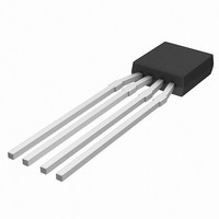
KMZ10C,112 NXP Semiconductors, KMZ10C,112 Datasheet - Page 25

KMZ10C,112
Manufacturer Part Number
KMZ10C,112
Description
IC MAGNETIC FIELD SENSOR SOT195
Manufacturer
NXP Semiconductors
Type
Special Purposer
Specifications of KMZ10C,112
Sensing Range
2mV/V
Voltage - Supply
5 V ~ 10 V
Output Type
Analog
Operating Temperature
-40°C ~ 150°C
Package / Case
SOT-195
Mounting Style
SMD/SMT
Maximum Operating Temperature
+ 150 C
Minimum Operating Temperature
- 40 C
Supply Voltage (min)
5 V
Supply Voltage (max)
10 V
Operating Temperature (min)
-40C
Operating Supply Voltage (typ)
5V
Lead Free Status / RoHS Status
Lead free / RoHS Compliant
Current - Supply
-
Current - Output (max)
-
Features
-
Lead Free Status / Rohs Status
Lead free / RoHS Compliant
Other names
933698480112
KMZ10C T/R
KMZ10C T/R
KMZ10C T/R
KMZ10C T/R
Philips Semiconductors
This circuit actually produces the necessary supply to
drive two flipping coils, which may be needed in some
applications such as an electronic compass (see Section
“Application examples”). Another separate clock or clock
generated by a P in the system could also be used to
drive TR1 and TR2.
The two resistors, R1 and R2, reduce the supply voltage of
the set-up down to the level required for the sensor bridge,
in this case reducing VCC = 10 V down to about 5 V. The
flipped output signal of the sensor bridge is amplified by
the pre-amplification circuit (Block 2) by a factor of 100,
providing a signal up to about 300 mV
about 15 A/m in the sensor plane). Of course, this voltage
would only be visible in un-compensated mode; when the
circuit is being used in compensated mode, this voltage
will be approximately 0 mV
1998 Jun 12
handbook, halfpage
a)
b)
Magnetic field sensors
V op
V o
(V)
(V)
0.25
0.5
0.5
1
0
0
0
0
PP
0.25
.
1
Fig.27 Oscillograph of flipping current in a MR sensor.
offset compensation response
PP
mag. pulse: 30 A/m
R3, R4 = 1.5 k
t/s
t/s
pulse response
(given a field of
0.5
MBH629
2
25
c)
Referring to the block diagram, Fig.26, the integrator
around IC2B in Block 3 provides the filtering to remove the
offset. In fact, in this set-up it is performed with a low pass
filter rather than high pass filtering. The low-pass filter
extracts the offset and uses it as negative feedback at
IC2A. It does not use the measured signal which, because
of the flipping, is now a signal modulated at the flipping
frequency. This has two main advantages:
The design of this filter affects system performance
significantly. In this example, the flipping frequency is
1 kHz with a filter roll off of 4 Hz.
handbook, halfpage
The op-amp in Block 2 is only amplifying the wanted
signal, allowing the gain to be higher with no overload
(or clipping) due to DC components.
The offset of the op-amp in Block 2 will also be
compensated, eliminating the need for special low offset
amplifiers, reducing overall system costs.
(A)
(A)
0.25
0.25
i F
i F
0.5
0.5
0
0
0
25
25
negative flip current
positive flip current
t/ s
t/ s
General
MBH666
50
50


