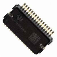
SCC1300-D04 VTI Technologies, SCC1300-D04 Datasheet - Page 12

SCC1300-D04
Manufacturer Part Number
SCC1300-D04
Description
GYRO/ACC COMBO 3-AXIS +/-6G SPI
Manufacturer
VTI Technologies
Datasheet
1.SCC1300-D04_PWB.pdf
(30 pages)
Specifications of SCC1300-D04
Output Type
Digital - SPI
Sensor Type
Gyroscope and Accelerometer
Lead Free Status / RoHS Status
Lead free / RoHS Compliant
Other names
551-1069-2
4
4.1 SPI Interfaces
4.2 Gyroscope Interface
4.2.1 SPI Transfer
Address Transfer:
VTI Technologies Oy
www.vti.fi
D15
0
Component Interfacing
D14
0
D13
0
SCC1300 sensor has two individual SPI interfaces for accelerometer and angular rate sensor that
need to be addressed separately. Both interfaces have their own four wire interconnection pins in
the component package. SPI communication transfers data between SPI master and registers of
the SCC1300 ASICs. SCC1300 ASICs always operate as slave devices in the master-slave
operation mode.
SCC1300 Angular rate sensor ASIC SPI interface:
SCC1300 Accelerometer ASIC SPI interface:
PLEASE NOTICE THAT EXACTLY THE SAME SPI ROUTINES DOES NOT WORK FOR BOTH
ASICS! E.g. SCC1300 accelerometer ASIC uses 8 bit addressing in SPI and SCC1300
angular rate sensor ASIC uses 16 bit addressing.
Both SPI interfaces and instructions to use them are explained separately in the following chapters.
This chapter describes the SCC1300 angular rate sensor ASIC interface and how to use it. The
angular rate sensor ASIC SPI interface has 16 bit addressing.
The SPI transfer is based on a 16-bit protocol. Figure 5 shows an example of a single 16-bit data
transmission. Each output data/status-bits are shifted out on the falling edge of SCK (MISO line).
Each bit is sampled on the rising edge of SCK (MOSI line).
Figure 5. SCC1300 angular rate sensor 16-bit data transmission.
After the falling edge of CSN_G the device interprets the first 16-bit word is an address transfer
having a bit coding scheme below.
MOSI_G
MISO_G
SCK_G
CSN_G
MOSI_A
MISO_A
SCK_A
CSB_A
D12
0
D11
0
D10
0
Doc.Nr. 82 1131 00 A
Subject to changes
D9
ADR6
master out slave in
master in slave out
serial clock
chip select (low active)
master out slave in
master in slave out
serial clock
chip select (low active)
D8
ADR5
D7
ADR4
D6
ADR3
D5
ADR2
D4
ADR1
D3
ADR0
µP → ASIC
ASIC → µP
µP → ASIC
µP → ASIC
µP → ASIC
ASIC → µP
µP → ASIC
µP → ASIC
D2
RW
0
D1
SCC1300-D04
D0
Par
odd
Rev. 1.0
12/30


