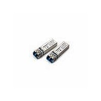
HFCT-5953TL Avago Technologies US Inc., HFCT-5953TL Datasheet - Page 2

HFCT-5953TL
Manufacturer Part Number
HFCT-5953TL
Description
Fiber Optic Transmitters, Receivers, Transceivers OC12 IR 2x5 SFF LC
Manufacturer
Avago Technologies US Inc.
Datasheet
1.HFCT-5953TL.pdf
(17 pages)
Specifications of HFCT-5953TL
Function
High performance, modules for serial optical data communication applications, designed for single mode fiber.
Product
Transceiver
Data Rate
622 Mbps
Wavelength
1300 nm
Maximum Rise Time
1 ns, 0.5 ns
Maximum Fall Time
1 ns, 0.5 ns
Maximum Output Current
50 mA
Operating Supply Voltage
3.14 V to 3.47 V
Maximum Operating Temperature
+ 70 C
Minimum Operating Temperature
0 C
Package / Case
DIP-10 with Connector
Optical Fiber Type
TX/RX
Data Transfer Rate
622Mbps
Optical Rise Time
1/0.5ns
Optical Fall Time
1/0.5ns
Operating Temperature Classification
Commercial
Peak Wavelength
1356/1570nm
Package Type
DIP With Connector
Operating Supply Voltage (min)
3.14V
Operating Supply Voltage (typ)
3.3V
Operating Supply Voltage (max)
3.47V
Output Current
50mA
Operating Temp Range
0C to 70C
Mounting
Snap Fit To Panel
Pin Count
10
For Use With
Singlemode Glass
Lead Free Status / RoHS Status
Lead free / RoHS Compliant
Functional Description
Receiver Section
Design
The receiver section contains an InGaAs/InP photo
detector and a preamplifier mounted in an optical
subassembly. This optical subassembly is coupled to a
postamp/decision circuit.
The postamplifier is ac coupled to the preamplifier as
illustrated in Figure 1. The coupling capacitors are large
enough to pass the SONET/SDH test pattern at 622 MBd
without significant distortion or performance penalty.
If a lower signal rate, or a code which has significantly
more low frequency content is used, sensitivity, jitter
and pulse distortion could be degraded.
Figure 1 also shows a filter function which limits the
bandwidth of the preamp output signal. The filter is de-
signed to bandlimit the preamp output noise and thus
improve the receiver sensitivity.
These components will reduce the sensitivity of the re-
ceiver as the signal bit rate is increased above 622 Mb/s.
The device incorporates a photodetector bias circuit.
This output must be connected to V
monitored by connecting through a series resistor (see
application section).
Figure 1 - Receiver Block Diagram
2
PHOTODETECTOR
BIAS
TRANS-
IMPEDANCE
PRE-
AMPLIFIER
GND
FILTER
CC
and can be
AMPLIFIER
CIRCUIT
SIGNAL
DETECT
Noise Immunity
The receiver includes internal circuit components to
filter power supply noise. However under some condi-
tions of EMI and power supply noise, external power
supply filtering may be necessary (see application sec-
tion).
The Signal Detect Circuit
The signal detect circuit works by sensing the peak level
of the received signal and comparing this level to a ref-
erence. The SD output is low voltage TTL.
PECL
OUTPUT
BUFFER
TTL
OUTPUT
BUFFER
DATA OUT
DATA OUT
SD


