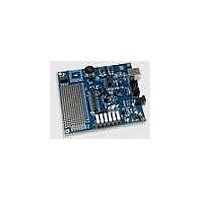
C8051F206DK-G Silicon Laboratories Inc, C8051F206DK-G Datasheet - Page 114

C8051F206DK-G
Manufacturer Part Number
C8051F206DK-G
Description
MCU, MPU & DSP Development Tools MCU DEVELOPMENT KIT W/ GLOBAL POWER SPLY
Manufacturer
Silicon Laboratories Inc
Datasheet
1.C8051F226DK.pdf
(146 pages)
Specifications of C8051F206DK-G
Processor To Be Evaluated
C8051F206
Data Bus Width
8 bit
Interface Type
USB
Lead Free Status / RoHS Status
Lead free / RoHS Compliant
- Current page: 114 of 146
- Download datasheet (2Mb)
C8051F2xx
114
Bit7:
Bit6:
Bits5–3: BC2–BC0: SPI Bit Count.
Bits2–0:
CKPHA
R/W
Bit7
CKPHA: SPI Clock Phase.
This bit controls the SPI clock phase.
0: Data sampled on first edge of SCK period.
1: Data sampled on second edge of SCK period.
CKPOL: SPI Clock Polarity.
This bit controls the SPI clock polarity.
0: SCK line low in idle state.
1: SCK line high in idle state.
Indicates which of the up to 8 bits of the SPI word have been transmitted.
These three bits determine the number of bits to shift in/out of the SPI shift register during a
data transfer in master mode. They are ignored in slave mode.
SPIFRS2–SPIFRS0: SPI Frame Size.
0
0
0
0
1
1
1
1
CKPOL
0
0
0
0
1
1
1
1
R/W
Bit6
BC2 – BC0
SPIFRS
SFR Definition 15.1. SPI0CFG: SPI Configuration
0
0
1
1
0
0
1
1
0
0
1
1
0
0
1
1
BC2
Bit5
R
0
1
0
1
0
1
0
1
0
1
0
1
0
1
0
1
BC1
Bit4
R
Bit Transmitted
Bits Shifted
Bit 7 (MSB)
Bit 0 (LSB)
Bit 1
Bit 2
Bit 3
Bit 4
Bit 5
Bit 6
1
2
3
4
5
6
7
8
Rev. 1.6
BC0
Bit3
R
SPIFRS2 SPIFRS1 SPIFRS0
R/W
Bit2
R/W
Bit1
R/W
Bit0
SFR Address:
Reset Value
00000111
0x9A
Related parts for C8051F206DK-G
Image
Part Number
Description
Manufacturer
Datasheet
Request
R
Part Number:
Description:
SMD/C°/SINGLE-ENDED OUTPUT SILICON OSCILLATOR
Manufacturer:
Silicon Laboratories Inc
Part Number:
Description:
Manufacturer:
Silicon Laboratories Inc
Datasheet:
Part Number:
Description:
N/A N/A/SI4010 AES KEYFOB DEMO WITH LCD RX
Manufacturer:
Silicon Laboratories Inc
Datasheet:
Part Number:
Description:
N/A N/A/SI4010 SIMPLIFIED KEY FOB DEMO WITH LED RX
Manufacturer:
Silicon Laboratories Inc
Datasheet:
Part Number:
Description:
N/A/-40 TO 85 OC/EZLINK MODULE; F930/4432 HIGH BAND (REV E/B1)
Manufacturer:
Silicon Laboratories Inc
Part Number:
Description:
EZLink Module; F930/4432 Low Band (rev e/B1)
Manufacturer:
Silicon Laboratories Inc
Part Number:
Description:
I°/4460 10 DBM RADIO TEST CARD 434 MHZ
Manufacturer:
Silicon Laboratories Inc
Part Number:
Description:
I°/4461 14 DBM RADIO TEST CARD 868 MHZ
Manufacturer:
Silicon Laboratories Inc
Part Number:
Description:
I°/4463 20 DBM RFSWITCH RADIO TEST CARD 460 MHZ
Manufacturer:
Silicon Laboratories Inc
Part Number:
Description:
I°/4463 20 DBM RADIO TEST CARD 868 MHZ
Manufacturer:
Silicon Laboratories Inc
Part Number:
Description:
I°/4463 27 DBM RADIO TEST CARD 868 MHZ
Manufacturer:
Silicon Laboratories Inc
Part Number:
Description:
I°/4463 SKYWORKS 30 DBM RADIO TEST CARD 915 MHZ
Manufacturer:
Silicon Laboratories Inc
Part Number:
Description:
N/A N/A/-40 TO 85 OC/4463 RFMD 30 DBM RADIO TEST CARD 915 MHZ
Manufacturer:
Silicon Laboratories Inc
Part Number:
Description:
I°/4463 20 DBM RADIO TEST CARD 169 MHZ
Manufacturer:
Silicon Laboratories Inc


