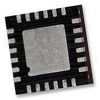
ITG-3200 INVENSENSE, ITG-3200 Datasheet - Page 17

ITG-3200
Manufacturer Part Number
ITG-3200
Description
IC, GYRO, TRI-AXIS, +/-2000 DEG/S
Manufacturer
INVENSENSE
Datasheet
1.ITG-3200.pdf
(39 pages)
Specifications of ITG-3200
No. Of Axes
3
Sensor Case Style
QFN
No. Of Pins
24
Supply Voltage Range
2.1V To 3.6V
Operating Temperature Range
-40°C To +85°C
Interface
I2C, Serial
Interface Type
I2C, Serial
Rohs Compliant
Yes
Lead Free Status / RoHS Status
Lead free / RoHS Compliant
Available stocks
Company
Part Number
Manufacturer
Quantity
Price
Part Number:
ITG-3200
Manufacturer:
INVENSE
Quantity:
20 000
5.4
The ITG-3200 communicates to a system processor using the I
when communicating to the system processor. The logic level for communications to the master is set by the
voltage on the VLOGIC pin. The LSB of the of the I
5.5
The ITG-3200 has a flexible clocking scheme, allowing for a variety of internal or external clock sources for the
internal synchronous circuitry. This synchronous circuitry includes the signal conditioning, ADCs, and various control
circuits and registers. An on-chip PLL provides flexibility in the allowable inputs for generating this clock.
Which source to select for generating the internal synchronous clock depends on the availability of external sources and
the requirements for clock accuracy. There are also start-up conditions to consider. When the ITG-3200 first starts up,
the device operates off of its internal clock until programmed to operate from another source. This allows the user, for
example, to wait for the MEMS oscillators to stabilize before they are selected as the clock source.
5.6
The sensor data registers contain the latest gyro and temperature data. They are read-only registers, and are accessed
via the Serial Interface. Data from these registers may be read at any time, however, the interrupt function may be used
to determine when new data is available.
5.7
Interrupt functionality is configured via the Interrupt Configuration register. Items that are configurable include the INT
pin configuration, the interrupt latching and clearing method, and triggers for the interrupt. Items that can trigger an
interrupt are (1) Clock generator locked to new reference oscillator (used when switching clock sources); and (2) new
data is available to be read from the Data registers. The interrupt status can be read from the Interrupt Status register.
5.8
An on-chip temperature sensor and ADC are used to measure the ITG-3200 die temperature. The readings from the
ADC can be read from the Sensor Data registers.
5.9
The bias and LDO sections take in an unregulated VDD supply from 2.1V to 3.6V and generate the internal supply and
the references voltages and currents required by the ITG-3200. The LDO output is bypassed by a capacitor at
REGOUT. Additionally, the part has a VLOGIC reference voltage which sets the logic levels for its I
5.10 Charge Pump
An on-board charge pump generates the high voltage (25V) required to drive the MEMS oscillators. Its output is
bypassed by a capacitor at CPOUT.
Allowable internal sources for generating the internal clock are:
Allowable external clocking sources are:
I
Clocking
Sensor Data Registers
Interrupts
Digital-Output Temperature Sensor
Bias and LDO
2
C Serial Communications Interface
An internal relaxation oscillator (less accurate)
Any of the X, Y, or Z gyros’ MEMS oscillators (with an accuracy of ±2% over temperature)
32.768kHz square wave
19.2MHz square wave
ITG-3200 Product Specification
2
C slave address is set by pin 9 (AD0).
2
C serial interface, and the device always acts as a slave
Document Number: PS-ITG-3200A-00-01.4
Revision: 1.4
Release Date: 03/30/2010
17 of 39
2
C interface.


