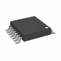
AD8367ARUZ-RL7 Analog Devices Inc, AD8367ARUZ-RL7 Datasheet - Page 3

AD8367ARUZ-RL7
Manufacturer Part Number
AD8367ARUZ-RL7
Description
IC,Voltage Controlled Gain Amplifier,SINGLE,TSSOP,14PIN,PLASTIC
Manufacturer
Analog Devices Inc
Series
X-AMP®r
Type
Variable Gain Amplifierr
Datasheet
1.AD8367-EVAL.pdf
(24 pages)
Specifications of AD8367ARUZ-RL7
Amplifier Type
Variable Gain
Number Of Circuits
1
-3db Bandwidth
500MHz
Current - Input Bias
27µA
Current - Supply
26mA
Voltage - Supply, Single/dual (±)
2.7 V ~ 5.5 V
Operating Temperature
-40°C ~ 85°C
Mounting Type
Surface Mount
Package / Case
14-TSSOP
Number Of Channels
1
Number Of Elements
1
Power Supply Requirement
Single
Voltage Gain Db
45dB
Input Resistance
0.000225@5VMohm
Input Bias Current
27@5VnA
Single Supply Voltage (typ)
3/5V
Dual Supply Voltage (typ)
Not RequiredV
Power Dissipation
250mW
Rail/rail I/o Type
No
Single Supply Voltage (min)
2.7V
Single Supply Voltage (max)
5.5V
Dual Supply Voltage (min)
Not RequiredV
Dual Supply Voltage (max)
Not RequiredV
Operating Temp Range
-40C to 85C
Operating Temperature Classification
Industrial
Mounting
Surface Mount
Pin Count
14
Package Type
TSSOP
Lead Free Status / RoHS Status
Lead free / RoHS Compliant
Output Type
-
Current - Output / Channel
-
Slew Rate
-
Gain Bandwidth Product
-
Voltage - Input Offset
-
Lead Free Status / Rohs Status
Compliant
Available stocks
Company
Part Number
Manufacturer
Quantity
Price
Part Number:
AD8367ARUZ-RL7
Manufacturer:
ADI/亚德诺
Quantity:
20 000
SPECIFICATIONS
V
Table 1.
Parameter
OVERALL FUNCTION
INPUT STAGE
GAIN CONTROL INTERFACE
OUTPUT STAGE
SQUARE LAW DETECTOR
POWER INTERFACE
MODE CONTROL INTERFACE
ENABLE INTERFACE
Frequency Range
GAIN Range
Maximum Input
Input Resistance
Scaling Factor
Gain Law Conformance
Maximum Gain
Minimum Gain
V
Small Signal Bandwidth
Maximum Output Voltage Swing
Output Source Resistance
Output Centering Voltage
Output Set Point
AGC Small Signal Response Time
Supply Voltage
Total Supply Current
Disable Current vs. Temperature
Mode LO Threshold
Mode HI Threshold
Enable Threshold
Enable Response Time
Enable Input Bias Current
f = 70 MHz
Gain
Gain Scaling Factor
Gain Intercept
Noise Figure
Output IP3
Output 1 dB Compression Point
S
GAIN
= 5 V, T
Step Response
A
= 25°C, system impedance Z
1
O
= 200 Ω, V
Conditions
Pins INPT and ICOM
To avoid input overload
From INPT to ICOM
Pin GAIN
V
V
100 mV ≤ V
V
V
From 0 dB to 30 dB
From 30 dB to 0 dB
V
Pin VOUT
R
R
Series resistance of output buffer
Pin DETO
C
Pins VPSI, VPSO, ICOM, and OCOM
ENBL high, maximum gain, R
(includes load current)
ENBL low
−40°C ≤ TA ≤ +85°C
Pin MODE
Device in negative slope mode of operation
Device in positive slope mode of operation
Pin ENBL
Time delay following LO to HI transition until
device meets full specifications.
ENBL at 5 V
ENBL at 0 V
Maximum gain
Minimum gain
Maximum gain
f1 = 70 MHz, f2 = 71 MHz, V
V
MODE
MODE
GAIN
GAIN
GAIN
L
L
AGC
GAIN
= 1 kΩ
= 200 Ω
= 100 pF, 6 dB gain step
= 0.95 V
= 0.05 V
= 0.5 V
= 0.5 V
= 5 V, 50 mV ≤ V
= 0 V, 50 mV ≤ V
MODE
GAIN
= 5 V, f = 10 MHz, unless otherwise noted.
≤ 900 mV
Rev. A | Page 3 of 24
GAIN
GAIN
≤ 950 mV
≤ 950 mV
GAIN
L
= 200 Ω
= 0.5 V
Min
LF
175
2.7
Typ
45
700
200
+20
−20
±0.2
+42.5
−2.5
300
300
5
4.3
3.5
50
V
354
1
26
1.3
1.2
1.4
2.5
1.5
27
32
+42.5
−3.7
19.9
−5.6
6.2
36.5
29.5
8.5
1.5
S
/2
Max
5.5
30
1.6
1.8
500
225
AD8367
Unit
MHz
dB
mV p-p
Ω
mV/dB
mV/dB
dB
dB
dB
ns
ns
MHz
V p-p
V p-p
Ω
V
mV rms
μs
V
mA
mA
mA
V
V
V
μs
μA
nA
dB
dB
mV/dB
dB
dB
dBm
dBV rms
dBm
dBV rms


