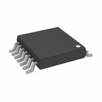
AD8367ARUZ-RL7 Analog Devices Inc, AD8367ARUZ-RL7 Datasheet - Page 4

AD8367ARUZ-RL7
Manufacturer Part Number
AD8367ARUZ-RL7
Description
IC,Voltage Controlled Gain Amplifier,SINGLE,TSSOP,14PIN,PLASTIC
Manufacturer
Analog Devices Inc
Series
X-AMP®r
Type
Variable Gain Amplifierr
Datasheet
1.AD8367-EVAL.pdf
(24 pages)
Specifications of AD8367ARUZ-RL7
Amplifier Type
Variable Gain
Number Of Circuits
1
-3db Bandwidth
500MHz
Current - Input Bias
27µA
Current - Supply
26mA
Voltage - Supply, Single/dual (±)
2.7 V ~ 5.5 V
Operating Temperature
-40°C ~ 85°C
Mounting Type
Surface Mount
Package / Case
14-TSSOP
Number Of Channels
1
Number Of Elements
1
Power Supply Requirement
Single
Voltage Gain Db
45dB
Input Resistance
0.000225@5VMohm
Input Bias Current
27@5VnA
Single Supply Voltage (typ)
3/5V
Dual Supply Voltage (typ)
Not RequiredV
Power Dissipation
250mW
Rail/rail I/o Type
No
Single Supply Voltage (min)
2.7V
Single Supply Voltage (max)
5.5V
Dual Supply Voltage (min)
Not RequiredV
Dual Supply Voltage (max)
Not RequiredV
Operating Temp Range
-40C to 85C
Operating Temperature Classification
Industrial
Mounting
Surface Mount
Pin Count
14
Package Type
TSSOP
Lead Free Status / RoHS Status
Lead free / RoHS Compliant
Output Type
-
Current - Output / Channel
-
Slew Rate
-
Gain Bandwidth Product
-
Voltage - Input Offset
-
Lead Free Status / Rohs Status
Compliant
Available stocks
Company
Part Number
Manufacturer
Quantity
Price
Part Number:
AD8367ARUZ-RL7
Manufacturer:
ADI/亚德诺
Quantity:
20 000
AD8367
Parameter
f = 140 MHz
f = 190 MHz
f = 240 MHz
1
The output dc centering voltage is normally set at V
Gain
Gain Scaling Factor
Gain Intercept
Noise Figure
Output IP3
Output 1 dB Compression Point
Gain
Gain Scaling Factor
Gain Intercept
Noise Figure
Output IP3
Output 1 dB Compression Point
Gain
Gain Scaling Factor
Gain Intercept
Noise Figure
Output IP3
Output 1 dB Compression Point
S
Conditions
Maximum gain
Minimum gain
Maximum gain
f1 = 140 MHz, f2 = 141 MHz, V
V
Maximum gain
Minimum gain
Maximum gain
f1 = 190 MHz, f2 = 191 MHz, V
V
Maximum gain
Minimum gain
Maximum gain
f1 = 240 MHz, f2 = 241 MHz, V
V
/2 and can be adjusted by applying a voltage to DECL.
GAIN
GAIN
GAIN
= 0.5 V
= 0.5 V
= 0.5 V
Rev. A | Page 4 of 24
GAIN
GAIN
GAIN
= 0.5 V
= 0.5 V
= 0.5 V
Min
Typ
+43.5
−3.6
19.7
−5.3
7.4
32.7
25.7
8.4
1.4
+43.5
−3.8
19.6
−5.3
7.5
30.9
23.9
8.4
1.4
+43
−4.1
19.7
−5.2
7.6
29.2
22.2
8.1
1.1
Max
Unit
dB
dB
mV/dB
dB
dB
dBm
dBV rms
dBm
dBV rms
dB
dB
mV/dB
dB
dB
dBm
dBV rms
dBm
dBV rms
dB
dB
mV/dB
dB
dB
dBm
dBV rms
dBm
dBV rms


