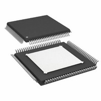
AD9272BSVZRL-40 Analog Devices Inc, AD9272BSVZRL-40 Datasheet - Page 13

AD9272BSVZRL-40
Manufacturer Part Number
AD9272BSVZRL-40
Description
12Bit 40 MSPS Octal ADC
Manufacturer
Analog Devices Inc
Type
Ultrasound Receiversr
Datasheet
1.AD9272BSVZ-80.pdf
(44 pages)
Specifications of AD9272BSVZRL-40
Design Resources
Powering AD9272 with ADP5020 Switching Regulator PMU for Increased Efficiency (CN0135)
Resolution (bits)
12 b
Sampling Rate (per Second)
40M
Data Interface
Serial
Voltage Supply Source
Analog and Digital
Voltage - Supply
1.8V, 3V
Operating Temperature
-40°C ~ 85°C
Mounting Type
Surface Mount
Package / Case
100-TQFP Exposed Pad, 100-eTQFP, 100-HTQFP, 100-VQFP
Lead Free Status / RoHS Status
Lead free / RoHS Compliant
For Use With
AD9272-65EBZ - BOARD EVAL AD9272
Lead Free Status / RoHS Status
Lead free / RoHS Compliant
Available stocks
Company
Part Number
Manufacturer
Quantity
Price
Company:
Part Number:
AD9272BSVZRL-40
Manufacturer:
Analog Devices Inc
Quantity:
10 000
Pin No.
20
23
24
27
28
29
30
31
32
33
34
35
36
37
38
39
40
41
42
43
44
45
46
48
49
51
52
53
56
57
58
59
62
63
64
65
68
69
70
71
74
75
76
77
78
79
80
81
82
83
84
85
87
Name
LG-H
CLK−
CLK+
DOUTH−
DOUTH+
DOUTG−
DOUTG+
DOUTF−
DOUTF+
DOUTE−
DOUTE+
DCO−
DCO+
FCO−
FCO+
DOUTD−
DOUTD+
DOUTC−
DOUTC+
DOUTB−
DOUTB+
DOUTA−
DOUTA+
STBY
PDWN
SCLK
SDIO
CSB
LG-A
LI-A
LOSW-A
LO-A
LG-B
LI-B
LOSW-B
LO-B
LG-C
LI-C
LOSW-C
LO-C
LG-D
LI-D
LOSW-D
LO-D
CWD0−
CWD0+
CWD1−
CWD1+
CWD2−
CWD2+
CWD3−
CWD3+
GAIN−
Description
LNA Ground for Channel H
Clock Input Complement
Clock Input True
ADC H Digital Output Complement
ADC H Digital Output True
ADC G Digital Output Complement
ADC G Digital Output True
ADC F Digital Output Complement
ADC F Digital Output True
ADC E Digital Output Complement
ADC E Digital Output True
Digital Clock Output Complement
Digital Clock Output True
Frame Clock Digital Output Complement
Frame Clock Digital Output True
ADC D Digital Output Complement
ADC D Digital Output True
ADC C Digital Output Complement
ADC C Digital Output True
ADC B Digital Output Complement
ADC B Digital Output True
ADC A Digital Output Complement
ADC A Digital Output True
Standby Power-Down
Full Power-Down
Serial Clock
Serial Data Input/Output
Chip Select Bar
LNA Ground for Channel A
LNA Analog Input for Channel A
LNA Analog Switched Output for Channel A
LNA Analog Inverted Output for Channel A
LNA Ground for Channel B
LNA Analog Input for Channel B
LNA Analog Switched Output for Channel B
LNA Analog Inverted Output for Channel B
LNA Ground for Channel C
LNA Analog Input for Channel C
LNA Analog Switched Output for Channel C
LNA Analog Inverted Output for Channel C
LNA Ground for Channel D
LNA Analog Input for Channel D
LNA Analog Switched Output for Channel D
LNA Analog Inverted Output for Channel D
CW Doppler Output Complement for Channel 0
CW Doppler Output True for Channel 0
CW Doppler Output Complement for Channel 1
CW Doppler Output True for Channel 1
CW Doppler Output Complement for Channel 2
CW Doppler Output True for Channel 2
CW Doppler Output Complement for Channel 3
CW Doppler Output True for Channel 3
Gain Control Voltage Input Complement
Rev. C | Page 13 of 44
AD9272


