AD9779BSVZRL Analog Devices Inc, AD9779BSVZRL Datasheet - Page 2
AD9779BSVZRL
Manufacturer Part Number
AD9779BSVZRL
Description
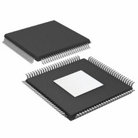
IC,D/A CONVERTER,DUAL,16-BIT,CMOS,TQFP,100PIN
Manufacturer
Analog Devices Inc
Datasheet
1.AD9776BSVZRL.pdf
(56 pages)
Specifications of AD9779BSVZRL
Number Of Bits
16
Data Interface
Serial
Number Of Converters
2
Voltage Supply Source
Analog and Digital
Power Dissipation (max)
300mW
Operating Temperature
-40°C ~ 85°C
Mounting Type
Surface Mount
Package / Case
100-TQFP Exposed Pad, 100-eTQFP, 100-HTQFP, 100-VQFP
Lead Free Status / RoHS Status
Lead free / RoHS Compliant
For Use With
AD9779A-EBZ - BOARD EVALUATION FOR AD9779A
Settling Time
-
Lead Free Status / RoHS Status
Lead free / RoHS Compliant
Available stocks
Company
Part Number
Manufacturer
Quantity
Price
Company:

Part Number:
AD9779BSVZRL
Manufacturer:
Analog Devices Inc
Quantity:
10 000


AD9776/AD9778/AD9779
TABLE OF CONTENTS
Features .............................................................................................. 1
Applications....................................................................................... 1
General Description ......................................................................... 1
Product Highlights ........................................................................... 1
Typical Signal Chain......................................................................... 1
Revision History ............................................................................... 2
Functional Block Diagram .............................................................. 3
Specifications..................................................................................... 4
Absolute Maximum Ratings............................................................ 8
Pin Configurations and Function Descriptions ........................... 9
Typical Performance Characteristics ........................................... 15
Terminology .................................................................................... 24
Theory of Operation ...................................................................... 25
REVISION HISTORY
3/07—Rev. 0 to Rev. A
Changes to Features.......................................................................... 1
Changes to Applications .................................................................. 1
Changes to General Product Highlights........................................ 1
Added Figure 1, Renumbered Figures Sequentially..................... 1
Changes to Table 1............................................................................ 4
Changes to Table 2............................................................................ 5
Changes to Table 3............................................................................ 5
Changes to Figure 53 and Figure 54............................................. 26
Changes to Table 12........................................................................ 29
Changes to Power Dissipation Section ........................................ 39
DC Specifications ......................................................................... 4
Digital Specifications ................................................................... 6
Digital Input Data Timing Specifications ................................. 7
AC Specifications.......................................................................... 7
Thermal Resistance ...................................................................... 8
ESD Caution.................................................................................. 8
Serial Peripheral Interface ......................................................... 25
MSB/LSB Transfers..................................................................... 26
Rev. A | Page 2 of 56
SPI Register Map ............................................................................ 27
Interpolation Filter Architecture .................................................. 31
Evaluation Board Operation ......................................................... 46
Outline Dimensions ....................................................................... 56
Added Table 19, Renumbered Tables Sequentially .................... 41
Changes to Figure 92 and Figure 93............................................. 42
Changes to Figure 94...................................................................... 42
Added New Figure 95, Renumbered Figures Sequentially ....... 42
Changes to Synchronization of Input Data to the REFCLK Input
(Pin 5 and Pin 6) with PLL Enabled or Disabled Section ......... 43
Added New Figure 96, Renumbered Figures Sequentially ....... 43
Changes to Figure 106 ................................................................... 51
7/05—Revision 0: Initial Version
Interpolation Filter Minimum and Maximum Bandwidth
Specifications .............................................................................. 35
Driving the REFCLK Input....................................................... 35
Internal PLL Clock Multiplier/Clock Distribution................ 36
Full-Scale Current Generation ................................................. 38
Power Dissipation....................................................................... 39
Power-Down and Sleep Modes................................................. 41
Interleaved Data Mode .............................................................. 41
Timing Information ................................................................... 41
Synchronization of Input Data to DATACLK
Output (Pin 37)........................................................................... 43
Synchronization of Input Data to the REFCLK Input (Pin 5
and Pin 6) with PLL Enabled or Disabled............................... 43
Modifying the Evaluation Board to Use the AD8349 On-
Board Quadrature Modulator................................................... 48
Evaluation Board Schematics ................................................... 49
Ordering Guide .......................................................................... 56
Related parts for AD9779BSVZRL
Image
Part Number
Description
Manufacturer
Datasheet
Request
R

Part Number:
Description:
16-Bit, 100 kSPS, Serial I/O A/D Converter
Manufacturer:
Analog Devices
Datasheet:

Part Number:
Description:
±1.7g Dual-Axis IMEMS Accelerometer Evaluation Board
Manufacturer:
Analog Devices Inc
Datasheet:

Part Number:
Description:
Inertial Sensor Evaluation System
Manufacturer:
Analog Devices Inc
Datasheet:
Part Number:
Description:
Manufacturer:
Analog Devices Inc
Datasheet:
Part Number:
Description:
Manufacturer:
Analog Devices Inc
Datasheet:
Part Number:
Description:
Manufacturer:
Analog Devices Inc
Datasheet:
Part Number:
Description:
Manufacturer:
Analog Devices Inc
Datasheet:
Part Number:
Description:
Manufacturer:
Analog Devices Inc
Datasheet:
Part Number:
Description:
Manufacturer:
Analog Devices Inc
Datasheet:
Part Number:
Description:
Manufacturer:
Analog Devices Inc
Datasheet:
Part Number:
Description:
Manufacturer:
Analog Devices Inc
Datasheet:
Part Number:
Description:
Manufacturer:
Analog Devices Inc
Datasheet:
Part Number:
Description:
Manufacturer:
Analog Devices Inc
Datasheet: