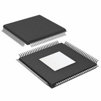
AD9779BSVZRL Analog Devices Inc, AD9779BSVZRL Datasheet - Page 29

AD9779BSVZRL
Manufacturer Part Number
AD9779BSVZRL
Description
IC,D/A CONVERTER,DUAL,16-BIT,CMOS,TQFP,100PIN
Manufacturer
Analog Devices Inc
Datasheet
1.AD9776BSVZRL.pdf
(56 pages)
Specifications of AD9779BSVZRL
Number Of Bits
16
Data Interface
Serial
Number Of Converters
2
Voltage Supply Source
Analog and Digital
Power Dissipation (max)
300mW
Operating Temperature
-40°C ~ 85°C
Mounting Type
Surface Mount
Package / Case
100-TQFP Exposed Pad, 100-eTQFP, 100-HTQFP, 100-VQFP
Lead Free Status / RoHS Status
Lead free / RoHS Compliant
For Use With
AD9779A-EBZ - BOARD EVALUATION FOR AD9779A
Settling Time
-
Lead Free Status / RoHS Status
Lead free / RoHS Compliant
Available stocks
Company
Part Number
Manufacturer
Quantity
Price
Company:
Part Number:
AD9779BSVZRL
Manufacturer:
Analog Devices Inc
Quantity:
10 000
Register Name
Sync Control Register
PLL Control
Misc Control
I DAC Control Register
Aux DAC1 Control
Register
Reg. No.
06
06
07
07
07
07
08
08
09
09
09
09
0A
0A
0B
0C
0C
0C
0D
0E
0E
0E
0E
Address
7:2
7:5
7
6
5
1:0
Bits
7:4
3:0
7
6
5
4:0
1:0
7
6:5
4:3
2:0
4:0
7:0
7
6
1:0
7:0
Description
Sync input delay
Input sync pulse timing error
tolerance
Sync receiver enable
Sync driver enable
Sync triggering edge
SYNC_I to input data sampling
clock offset
PLL band select
VCO AGC gain control
PLL enable
PLL VCO divide ratio
PLL loop divide ratio
PLL bias setting
PLL control voltage range
PLL loop bandwidth adjustment
I DAC gain adjustment
I DAC sleep
I DAC power-down
I DAC gain adjustment
Aux DAC1 gain adjustment
Aux DAC1 sign
Aux DAC1 current direction
Aux DAC1 power-down
Aux DAC1 gain adjustment
Rev. A | Page 29 of 56
Function
See the Multiple DAC Synchronization
section for details on using these registers
to synchronize multiple DACs
VCO frequency range vs. PLL band select
value (see Table 18)
Lower number (low gain) is generally better
for performance
0: PLL off, DAC rate clock supplied by
outside source
1: PLL on, DAC rate clock synthesized
internally from external reference clock via
PLL clock multiplier
FVCO/f
f
Always set to 010
000 to 111, proportional to voltage at PLL
loop filter output, readback only
See PLL Loop Filter Bandwidth section for
details
(7:0) LSB slice of 10-bit gain setting word
for I DAC
0: I DAC on
1: I DAC off
0: I DAC on
1: I DAC off
(9:8) MSB slice of 10-bit gain setting word
for I DAC
(7:0) LSB slice of 10-bit gain setting word for
Aux DAC1
0: positive
1: negative
0: source
1: sink
0: Aux DAC1 on
1: Aux DAC1 off
(9:8) MSB slice of 10-bit gain setting word
for Aux DAC1
DAC
00 × 1
01 × 2
10 × 4
11 × 8
00 × 2
01 × 4
10 × 8
11 × 16
/f
REF
DAC
AD9776/AD9778/AD9779
Default
0
0
0
0
0
0
111001
11
0
010
11111001
0
0
01
00000000
0
0
00


