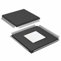
AD9779BSVZRL Analog Devices Inc, AD9779BSVZRL Datasheet - Page 44

AD9779BSVZRL
Manufacturer Part Number
AD9779BSVZRL
Description
IC,D/A CONVERTER,DUAL,16-BIT,CMOS,TQFP,100PIN
Manufacturer
Analog Devices Inc
Datasheet
1.AD9776BSVZRL.pdf
(56 pages)
Specifications of AD9779BSVZRL
Number Of Bits
16
Data Interface
Serial
Number Of Converters
2
Voltage Supply Source
Analog and Digital
Power Dissipation (max)
300mW
Operating Temperature
-40°C ~ 85°C
Mounting Type
Surface Mount
Package / Case
100-TQFP Exposed Pad, 100-eTQFP, 100-HTQFP, 100-VQFP
Lead Free Status / RoHS Status
Lead free / RoHS Compliant
For Use With
AD9779A-EBZ - BOARD EVALUATION FOR AD9779A
Settling Time
-
Lead Free Status / RoHS Status
Lead free / RoHS Compliant
Available stocks
Company
Part Number
Manufacturer
Quantity
Price
Company:
Part Number:
AD9779BSVZRL
Manufacturer:
Analog Devices Inc
Quantity:
10 000
AD9776/AD9778/AD9779
Using Data Delay to Meet Timing Requirements
To meet strict timing requirements at input data rates of up to
250 MSPS, the AD977x has a fine timing feature. Fine timing
adjustments are made by programming values into the data
clock delay register (Register 0x04, Bits<7:4>). This register can
be used to add delay between the REFCLK in and the
DATACLK out. Figure 97 shows the default delay present when
DATACLK delay is disabled. The disable function bit is found
in Register 0x02, Bit 4. Figure 98 shows the delay present when
DATACLK delay is enabled and set to 0000. Figure 99 indicates
the delay when DATACLK delay is enabled and set to 1111.
Note that the setup and hold times specified for data to
DATACLK are defined for DATACLK delay disabled.
Figure 98. Delay from REFCLK to DATACLK Out with DATACLK Delay = 0000
TEK RUN: 5.00GS/s
TEK RUN: 5.00GS/s
2
1
2
1
Figure 97. Delay from REFCLK to DATACLK with DATACLK Delay Disabled
CH1 1.00VΩ
CH1 1.00V Ω
CH2
CH2
SAMPLE
SAMPLE
500mVΩ
500mV Ω
M2.00ns
M2.00ns
CH1
CH1
420mV
420mV
Δ: 4.48nS
@: 40.28nS
Δ : 4.76nS
@: 35.52nS
Rev. A | Page 44 of 56
The difference between the minimum delay shown in Figure 98
and the maximum delay shown in Figure 99 is the range
programmable using the DATACLK delay register. The delay
(in absolute time) when programming DATACLK delay
between 0000 and 1111 is a linear extrapolation between these
two figures. The typical delays per increment over temperature
are shown in Table 20.
Table 20. Data Delay Line Typical Delays Over Temperature
Delays
Delay Between Disabled and
Enabled
Average Delay per Increment
The frequency of DATACLK out depends on several program-
mable settings: interpolation, zero stuffing, and interleaved/
dual port mode, all of which have an effect on the REFCLK
frequency. The divisor function between REFCLK and
DATACLK is equal to the values shown in Table 21.
Table 21. REFCLK to DATACLK Divisor Ratio
Interpolation
1
2
4
8
1
2
4
8
1
2
4
8
1
2
4
8
Figure 99. Delay from REFCLK to DATACLK Out with DATACLK Delay = 1111
TEK RUN: 5.00GS/s
2
1
CH1 1.00V Ω
CH2
Zero Stuffing
Disabled
Disabled
Disabled
Disabled
Disabled
Disabled
Disabled
Disabled
Enabled
Enabled
Enabled
Enabled
Enabled
Enabled
Enabled
Enabled
SAMPLE
500mV Ω
M2.00ns
−40°C
370
171
Input Mode
Dual port
Dual port
Dual port
Dual port
Interleaved
Interleaved
Interleaved
Interleaved
Dual port
Dual port
Dual port
Dual port
Interleaved
Interleaved
Interleaved
Interleaved
CH1
+25°C
416
183
420mV
+85°C
432
197
Δ : 7.84nS
@: 32.44nS
Divisor
1
2
4
8
Invalid
1
2
4
2
4
8
16
1
2
4
8
Unit
ps
ps


