AD9779BSVZRL Analog Devices Inc, AD9779BSVZRL Datasheet - Page 28
AD9779BSVZRL
Manufacturer Part Number
AD9779BSVZRL
Description
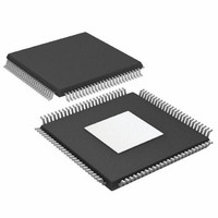
IC,D/A CONVERTER,DUAL,16-BIT,CMOS,TQFP,100PIN
Manufacturer
Analog Devices Inc
Datasheet
1.AD9776BSVZRL.pdf
(56 pages)
Specifications of AD9779BSVZRL
Number Of Bits
16
Data Interface
Serial
Number Of Converters
2
Voltage Supply Source
Analog and Digital
Power Dissipation (max)
300mW
Operating Temperature
-40°C ~ 85°C
Mounting Type
Surface Mount
Package / Case
100-TQFP Exposed Pad, 100-eTQFP, 100-HTQFP, 100-VQFP
Lead Free Status / RoHS Status
Lead free / RoHS Compliant
For Use With
AD9779A-EBZ - BOARD EVALUATION FOR AD9779A
Settling Time
-
Lead Free Status / RoHS Status
Lead free / RoHS Compliant
Available stocks
Company
Part Number
Manufacturer
Quantity
Price
Company:

Part Number:
AD9779BSVZRL
Manufacturer:
Analog Devices Inc
Quantity:
10 000


AD9776/AD9778/AD9779
Table 12. SPI Register Description
Register Name
Comm Register
Digital Control Register
Sync Control Register
Reg. No.
00
00
00
00
00
00
01
01
01
02
02
02
02
02
02
02
02
03
03
03
04
04
04
05
05
05
Address
Bits
7
6
5
4
3
1
7:6
5:2
0
7
6
5
4
3
2
1
0
7:6
5:4
3:0
7:4
3:1
0
7:4
3:1
0
Description
SDIO bidirectional
LSB/MSB first
Software reset
Power-down mode
Auto power-down enable
PLL lock (read only)
Filter interpolation factor
Filter modulation mode
Zero stuffing
Data format
Dual/interleaved data bus mode
Real mode
DATACLK delay enable
Inverse sinc enable
DATACLK invert
TxEnable invert
Q first
Data clock delay mode
Extra data clock divide ratio
Reserved
Data clock delay
Output sync pulse divide
Sync out delay
Sync out delay
Input sync pulse frequency
Sync input delay
Rev. A | Page 28 of 56
Function
0: use SDIO pin as input data only
1: use SDIO as both input and output data
0: first bit of serial data is MSB of data byte
1: first bit of serial data is LSB of data byte
Bit must be written with a 1, then 0 to soft
reset SPI register map
0: all circuitry is active
1: disable all digital and analog circuitry,
only SPI port is active
Controls auto power-down mode, see the
Power-Down and Sleep Modes section
0: PLL is not locked
1: PLL is locked
00: 1× interpolation
01: 2× interpolation
10: 4× interpolation
11: 8× interpolation
See Table 21 for filter modes
0: zero stuffing off
1: zero stuffing on
0: signed binary
1: unsigned binary
0: both input data ports receive data
1: Data Port 1 only receives data
0: enable Q path for signal processing
1: disable Q path data (internal Q channel
clocks disabled, I and Q modulators
disabled)
See the Using Data Delay to Meet Timing
Requirements section.
0: inverse sinc filter disabled
1: inverse sinc filter enabled
0: output DATACLK same phase as internal
capture clock
1: output DATACLK opposite phase as
internal capture clock
Inverts the function of TxEnable Pin 39, see
the Interleaved Data Mode section
0: first byte of data is always I data at
beginning of transmit
1: first byte of data is always Q data at
beginning of transmit
00: manual
Data clock output divider (see Table 22 for
divider ratio)
Sets delay of REFCLK in to DATACLK out
Sets frequency of SYNC_O pulses
Sync output delay, Bit 4
Sync output delay, Bits<3:0>
Input sync pulse frequency divider, see the
AN-822
Sync input delay, Bit 4
application note
Default
0
0
0
0
0
00
0000
0
0
0
0
0
0
0
00
00
000
0000
000
0
000
0
Related parts for AD9779BSVZRL
Image
Part Number
Description
Manufacturer
Datasheet
Request
R

Part Number:
Description:
16-Bit, 100 kSPS, Serial I/O A/D Converter
Manufacturer:
Analog Devices
Datasheet:

Part Number:
Description:
±1.7g Dual-Axis IMEMS Accelerometer Evaluation Board
Manufacturer:
Analog Devices Inc
Datasheet:

Part Number:
Description:
Inertial Sensor Evaluation System
Manufacturer:
Analog Devices Inc
Datasheet:
Part Number:
Description:
Manufacturer:
Analog Devices Inc
Datasheet:
Part Number:
Description:
Manufacturer:
Analog Devices Inc
Datasheet:
Part Number:
Description:
Manufacturer:
Analog Devices Inc
Datasheet:
Part Number:
Description:
Manufacturer:
Analog Devices Inc
Datasheet:
Part Number:
Description:
Manufacturer:
Analog Devices Inc
Datasheet:
Part Number:
Description:
Manufacturer:
Analog Devices Inc
Datasheet:
Part Number:
Description:
Manufacturer:
Analog Devices Inc
Datasheet:
Part Number:
Description:
Manufacturer:
Analog Devices Inc
Datasheet:
Part Number:
Description:
Manufacturer:
Analog Devices Inc
Datasheet:
Part Number:
Description:
Manufacturer:
Analog Devices Inc
Datasheet: