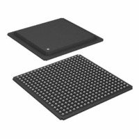
ADSP-21160NCB-100 Analog Devices Inc, ADSP-21160NCB-100 Datasheet - Page 13

ADSP-21160NCB-100
Manufacturer Part Number
ADSP-21160NCB-100
Description
IC,DSP,32-BIT,CMOS,BGA,400PIN,PLASTIC
Manufacturer
Analog Devices Inc
Series
SHARC®r
Type
Floating Pointr
Specifications of ADSP-21160NCB-100
Rohs Status
RoHS non-compliant
Interface
Host Interface, Link Port, Serial Port
Clock Rate
100MHz
Non-volatile Memory
External
On-chip Ram
512kB
Voltage - I/o
3.30V
Voltage - Core
1.90V
Operating Temperature
-40°C ~ 100°C
Mounting Type
Surface Mount
Package / Case
400-BGA
Package
400BGA
Numeric And Arithmetic Format
Floating-Point
Maximum Speed
100 MHz
Ram Size
512 KB
Device Million Instructions Per Second
100 MIPS
Lead Free Status / RoHS Status
Available stocks
Company
Part Number
Manufacturer
Quantity
Price
Company:
Part Number:
ADSP-21160NCB-100
Manufacturer:
Analog Devices Inc
Quantity:
10 000
Table 3. Pin Function Descriptions (Continued)
Pin
ID2–0
DMAG1
DMAG2
BR6–1
RPBA
PA
DTx
DRx
TCLKx
RCLKx
TFSx
RFSx
LxDAT7–0
LxCLK
LxACK
EBOOT
LBOOT
BMS
CLKIN
CLK_CFG3–0
Type
I
O/T
O/T
I/O/S
I/S
I/O/T
O
I
I/O
I/O
I/O
I/O
I/O
I/O
I/O
I
I
I/O/T
I
I
Function
Multiprocessing ID. Determines which multiprocessing bus request (BR1–BR6) is used by the
ADSP-21160x. ID = 001 corresponds to BR1, ID = 010 corresponds to BR2, and so on. Use ID = 000
or ID = 001 in single-processor systems. These lines are a system configuration selection which
should be hardwired or only changed at reset.
DMA Grant 1 (DMA Channel 11). Asserted by ADSP-21160x to indicate that the requested DMA
starts on the next cycle. Driven by bus master only. DMAG1 has a 20 kΩ internal pull-up resistor
that is enabled on the ADSP-21160x with ID2–0 = 00x.
DMA Grant 2 (DMA Channel 12). Asserted by ADSP-21160x to indicate that the requested DMA
starts on the next cycle. Driven by bus master only. DMAG2 has a 20 kΩ internal pull-up resistor
that is enabled on the ADSP-21160x with ID2–0 = 00x.
Multiprocessing Bus Requests. Used by multiprocessing ADSP-21160x DSPs to arbitrate for bus
mastership. An ADSP-21160x only drives its own BRx line (corresponding to the value of its ID2–0
inputs) and monitors all others. In a multiprocessor system with less than six ADSP-21160x DSPs,
the unused BRx pins should be pulled high; the processor’s own BRx line must not be pulled high
or low because it is an output.
Rotating Priority Bus Arbitration Select. When RPBA is high, rotating priority for multiprocessor bus
arbitration is selected. When RPBA is low, fixed priority is selected. This signal is a system configu-
ration selection which must be set to the same value on every ADSP-21160x. If the value of RPBA
is changed during system operation, it must be changed in the same CLKIN cycle on every
processor.
Priority Access. Asserting its PA pin allows an ADSP-21160x bus slave to interrupt background DMA
transfers and gain access to the external bus. PA is connected to all ADSP-21160x DSPs in the system.
If access priority is not required in a system, the PA pin should be left unconnected. PA has a 20 kΩ
internal pull-up resistor that is enabled on the ADSP-21160x with ID2–0 = 00x.
Data Transmit (Serial Ports 0, 1). Each DT pin has a 50 kΩ internal pull-up resistor.
Data Receive (Serial Ports 0, 1). Each DR pin has a 50 kΩ internal pull-up resistor.
Transmit Clock (Serial Ports 0, 1). Each TCLK pin has a 50 kΩ internal pull-up resistor.
Receive Clock (Serial Ports 0, 1). Each RCLK pin has a 50 kΩ internal pull-up resistor.
Transmit Frame Sync (Serial Ports 0, 1).
Receive Frame Sync (Serial Ports 0, 1).
Link Port Data (Link Ports 0–5). Each LxDAT pin has a 50 kΩ internal pull-down resistor that is
enabled or disabled by the LPDRD bit of the LCTL0–1 register.
Link Port Clock (Link Ports 0–5). Each LxCLK pin has a 50 kΩ internal pull-down resistor that is
enabled or disabled by the LPDRD bit of the LCTL0–1 register.
Link Port Acknowledge (Link Ports 0–5). Each LxACK pin has a 50 kΩ internal pull-down resistor
that is enabled or disabled by the LPDRD bit of the LCOM register.
EPROM Boot Select. For a description of how this pin operates, see
configuration selection that should be hardwired.
Link Boot. For a description of how this pin operates, see
ration selection that should be hardwired.
Boot Memory Select. Serves as an output or input as selected with the EBOOT and LBOOT pins; see
Table
Local Clock In. CLKIN is the ADSP-21160x clock input. The ADSP-21160x external port cycles at the
frequency of CLKIN. The instruction cycle rate is a multiple of the CLKIN frequency; it is program-
mable at power-up. CLKIN may not be halted, changed, or operated below the specified frequency.
Core/CLKIN Ratio Control. ADSP-21160x core clock (instruction cycle) rate is equal to n x CLKIN
where n is user-selectable to 2, 3, or 4, using the CLK_CFG3–0 inputs. For clock configuration defini-
tions, see the RESET & CLKIN section of the System Design chapter of the ADSP-21160 SHARC DSP
Hardware Reference.
4. This input is a system configuration selection that should be hardwired.
Rev. B | Page 13 of 60 | February 2010
ADSP-21160M/ADSP-21160N
Table
4. This signal is a system configu-
Table
4. This signal is a system


