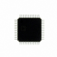
ADUC7060BSTZ32 Analog Devices Inc, ADUC7060BSTZ32 Datasheet - Page 56

ADUC7060BSTZ32
Manufacturer Part Number
ADUC7060BSTZ32
Description
DUAL 24-BIT AFE AND ARM 7 I.C
Manufacturer
Analog Devices Inc
Series
MicroConverter® ADuC7xxxr
Specifications of ADUC7060BSTZ32
Design Resources
4 mA-to-20 mA Loop-Powered Temperature Monitor Using ADuC7060/1 (CN0145) Low power, Long Range, ISM Wireless Measuring Node (CN0164)
Core Processor
ARM7
Core Size
16/32-Bit
Speed
10MHz
Connectivity
I²C, SPI, UART/USART
Peripherals
POR, PWM, Temp Sensor, WDT
Number Of I /o
14
Program Memory Size
32KB (16K x 16)
Program Memory Type
FLASH
Ram Size
4K x 8
Voltage - Supply (vcc/vdd)
2.375 V ~ 2.625 V
Data Converters
A/D 5x24b, 8x24b, D/A 1x14b
Oscillator Type
Internal
Operating Temperature
-40°C ~ 125°C
Package / Case
48-LQFP
Cpu Family
ADuC7xxx
Device Core
ARM7TDMI
Device Core Size
16/32Bit
Frequency (max)
10.24MHz
Interface Type
I2C/SPI/UART
Total Internal Ram Size
4KB
# I/os (max)
14
Number Of Timers - General Purpose
4
Operating Supply Voltage (typ)
2.5V
Operating Supply Voltage (max)
2.625V
Operating Supply Voltage (min)
2.375V
On-chip Adc
2(4-chx24-bit)
Instruction Set Architecture
RISC
Operating Temp Range
-40C to 125C
Operating Temperature Classification
Automotive
Mounting
Surface Mount
Pin Count
48
Package Type
LQFP
Package
48LQFP
Family Name
ADuC7xxx
Maximum Speed
10.24 MHz
Operating Supply Voltage
2.5 V
Data Bus Width
16|32 Bit
Number Of Programmable I/os
14
Number Of Timers
4
Lead Free Status / RoHS Status
Lead free / RoHS Compliant
Eeprom Size
-
Lead Free Status / Rohs Status
Compliant
Available stocks
Company
Part Number
Manufacturer
Quantity
Price
Company:
Part Number:
ADUC7060BSTZ32
Manufacturer:
CYPRESS
Quantity:
294
Company:
Part Number:
ADUC7060BSTZ32
Manufacturer:
ADI
Quantity:
315
Company:
Part Number:
ADUC7060BSTZ32
Manufacturer:
Analog Devices Inc
Quantity:
10 000
Part Number:
ADUC7060BSTZ32
Manufacturer:
ADI/亚德诺
Quantity:
20 000
Company:
Part Number:
ADUC7060BSTZ32-RL
Manufacturer:
Analog Devices Inc
Quantity:
10 000
ADuC7060/ADuC7061
DAC PERIPHERALS
DAC
The ADuC706x incorporates a voltage output DAC on chip. In
normal mode, the DAC resolution is 12-bits. In interpolation,
the DAC resolution is 16 bits with 14 effective bits. The DAC
has a rail-to-rail voltage output buffer capable of driving
5 kΩ/100 pF.
The DAC has four selectable ranges.
•
•
•
•
The maximum signal range is 0 V to AVDD.
Table 63. DAC0CON MMR Bit Designations
Bit
15:10
9
8
7
6
5
4
3
2
1:0
0 V to V
VREF− to VREF+
ADC5/EXT_REF2IN− to ADC4/EXT_REF2IN+
0 V to AVDD
Name
DACPD
DACBUFLP
OPAMP
DACBUFBYPASS
DACCLK
DACCLR
DACMODE
Rate
DAC range bits
REF
(internal band gap 1.2 V reference)
Reserved.
Set to 1 to enable the DAC in 16-bit interpolation mode.
Description
Set to 1 to power down DAC output (DAC output is tristated).
Clear this bit to enable the DAC.
Set to 1 to place the DAC output buffer in low power mode. See the Normal DAC Mode and Op Amp Mode
sections for further details on electrical specifications.
Clear this bit to enable the DAC buffer.
Set to 1 to place the DAC output buffer in op amp mode.
Clear this bit to enable the DAC output buffer for normal DAC operation.
Set to 1 to bypass the output buffer and send the DAC output directly to the output pin.
Clear this bit to buffer the DAC output.
Cleared to 0 to update the DAC on the negative edge of HCLK.
Set to 1 to update the DAC on the negative edge of Timer1. This mode is ideally suited for waveform generation
where the next value in the waveform is written to DAC0DAT at regular intervals of Timer1.
Set to 1 for normal DAC operation.
Set to 0 to clear the DAC output and to set DAC0DAT to 0. Writing to this bit has an immediate effect on the DAC
output.
Set to 0 to enable the DAC in normal 12-bit mode.
Used with interpolation mode.
Set to 1 to configure the interpolation clock as UCLK/16.
Set to 0 to configure the interpolation clock as UCLK/32.
[11] = 0 V to AVDD range.
[10] = ADC5/EXT_REF2IN− to ADC4/EXT_REF2IN+.
[01] = VREF− to VREF+.
[00] = 0 V to V
REF
(1.2 V) range. Internal reference source.
Rev. C | Page 56 of 108
Op Amp Mode
As an option, the DAC can be disabled and its output buffer
used as an op amp.
MMR INTERFACE
The DAC is configurable through a control register and a data
register.
DAC0CON Register
Name:
Address:
Default value:
Access:
DAC0CON
0x0200
Read and write
0xFFFF0600


