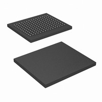
CY7C1412AV18-200BZC Cypress Semiconductor Corp, CY7C1412AV18-200BZC Datasheet - Page 18

CY7C1412AV18-200BZC
Manufacturer Part Number
CY7C1412AV18-200BZC
Description
SRAM (Static RAM)
Manufacturer
Cypress Semiconductor Corp
Datasheet
1.CY7C1412AV18-200BZXC.pdf
(27 pages)
Specifications of CY7C1412AV18-200BZC
Format - Memory
RAM
Memory Type
SRAM - Synchronous, QDR II
Memory Size
36M (2M x 18)
Speed
200MHz
Interface
Parallel
Voltage - Supply
1.7 V ~ 1.9 V
Operating Temperature
0°C ~ 70°C
Package / Case
165-TFBGA
Lead Free Status / RoHS Status
Contains lead / RoHS non-compliant
Available stocks
Company
Part Number
Manufacturer
Quantity
Price
Company:
Part Number:
CY7C1412AV18-200BZC
Manufacturer:
Cypress Semiconductor Corp
Quantity:
10 000
Maximum Ratings
Exceeding maximum ratings may impair the useful life of the
device. These user guidelines are not tested.
Storage Temperature ............................... –65 C to +150 C
Ambient Temperature with Power Applied –55 C to +125 C
Supply Voltage on V
Supply Voltage on V
DC Applied to Outputs in High Z ........ –0.5V to V
DC Input Voltage
Current into Outputs (LOW)......................................... 20 mA
Static Discharge Voltage (MIL-STD-883, M. 3015).. > 2001V
Latch-up Current.................................................... > 200 mA
Operating Range
Electrical Characteristics
DC Electrical Characteristics
Over the Operating Range
Notes
Document #: 38-05615 Rev. *H
V
V
V
V
V
V
V
V
I
I
V
I
15. Power up: Assumes a linear ramp from 0V to V
16. Output are impedance controlled. I
17. Output are impedance controlled. I
18. V
19. The operation current is calculated with 50% read cycle and 50% write cycle.
Commercial
Industrial
X
OZ
DD
Parameter
DD
DDQ
OH
OL
OH(LOW)
OL(LOW)
IH
IL
REF
[19]
Range
REF
(min) = 0.68V or 0.46V
Power Supply Voltage
IO Supply Voltage
Output HIGH Voltage
Output LOW Voltage
Output HIGH Voltage
Output LOW Voltage
Input HIGH Voltage
Input LOW Voltage
Input Leakage Current
Output Leakage Current
Input Reference Voltage
V
DD
[11]
Temperature (T
Operating Supply
–40°C to +85°C
DD
DDQ
0°C to +70°C
.............................. –0.5V to V
Description
Ambient
Relative to GND ........–0.5V to +2.9V
Relative to GND.......–0.5V to +V
DDQ
[12]
, whichever is larger, V
OH
OL
= (V
=
A
)
(V
DDQ
DDQ
[18]
/2)/(RQ/5) for values of 175 ohms <= RQ <= 350 ohms.
1.8 ± 0.1V
DD
/2)/(RQ/5) for values of 175 ohms <= RQ <= 350 ohms.
V
(min) within 200 ms. During this time V
DD
Note 16
Note 17
I
I
GND V
GND V
Typical Value = 0.75V
V
I
f = f
OH
OL
OUT
DD
[15]
REF
= 0.1 mA, Nominal Impedance
=0.1 mA, Nominal Impedance
MAX
= Max,
= 0 mA,
DDQ
(max) = 0.95V or 0.54V
DD
= 1/t
V
I
I
1.4V to
+ 0.3V
+ 0.3V
V
V
DDQ
V
Test Conditions
CYC
DD
DDQ
DDQ,
DD
[15]
Output Disabled
Neutron Soft Error Immunity
DDQ
LSBU
LMBU
SEL
* No LMBU or SEL events occurred during testing; this column represents a
statistical
cation Note
Terrestrial Failure Rates”
Parameter
250MHz (x18)
200MHz (x18)
167MHz (x18)
, whichever is smaller.
IH
< V
DD
2
, 95% confidence limit calculation. For more details refer to Appli-
AN54908 “Accelerated Neutron SER Testing and Calculation of
and V
(x36)
(x36)
(x36)
Logical Multi
Single Event
Description
DDQ
Bit Upsets
Single Bit
Latch up
Logical
Upsets
V
V
< V
DDQ
DDQ
V
V
DDQ
REF
DD
–0.3
0.68
Min
V
.
1.7
1.4
/2 – 0.12
/2 – 0.12
5
5
SS
+ 0.1
– 0.2
Test Con-
ditions
25°C
25°C
85°C
0.75
Typ
1.8
1.5
CY7C1412AV18
CY7C1414AV18
V
V
Typ
320
DDQ
DDQ
V
V
0
0
DDQ
REF
V
1000
Max
0.95
V
850
725
850
650
740
1.9
/2 + 0.12
/2 + 0.12
0.2
DDQ
DD
5
5
– 0.1
+ 0.3
Page 18 of 27
Max*
0.01
368
0.1
Unit
Unit
FIT/
FIT/
FIT/
Dev
mA
Mb
Mb
A
A
V
V
V
V
V
V
V
V
V
[+] Feedback


