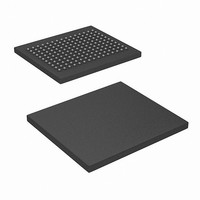
CY7C1412AV18-200BZC Cypress Semiconductor Corp, CY7C1412AV18-200BZC Datasheet - Page 22

CY7C1412AV18-200BZC
Manufacturer Part Number
CY7C1412AV18-200BZC
Description
SRAM (Static RAM)
Manufacturer
Cypress Semiconductor Corp
Datasheet
1.CY7C1412AV18-200BZXC.pdf
(27 pages)
Specifications of CY7C1412AV18-200BZC
Format - Memory
RAM
Memory Type
SRAM - Synchronous, QDR II
Memory Size
36M (2M x 18)
Speed
200MHz
Interface
Parallel
Voltage - Supply
1.7 V ~ 1.9 V
Operating Temperature
0°C ~ 70°C
Package / Case
165-TFBGA
Lead Free Status / RoHS Status
Contains lead / RoHS non-compliant
Available stocks
Company
Part Number
Manufacturer
Quantity
Price
Company:
Part Number:
CY7C1412AV18-200BZC
Manufacturer:
Cypress Semiconductor Corp
Quantity:
10 000
Switching Characteristics
Over the Operating Range
Notes
Document #: 38-05615 Rev. *H
Parameter
t
t
t
t
t
t
Setup Times
t
t
t
t
Hold Times
t
t
t
t
Output Times
t
t
t
t
t
t
t
t
DLL Timing
t
t
21. When a part with a maximum frequency above 167 MHz is operating at a lower clock frequency, it requires the input timing of the frequency range in which it is being
22. This part has a voltage regulator internally; t
23. For D2 data signal on CY7C1425AV18 device, t
24. t
25. At any voltage and temperature t
POWER
CYC
KH
KL
KHKH
KHCH
SA
SC
SCDDR
SD
HA
HC
HCDDR
HD
CO
DOH
CCQO
CQOH
CQD
CQDOH
CHZ
CLZ
KC Var
KC lock
Cypress
operated and outputs data with the output timings of that frequency range.
state voltage.
[23]
CHZ
, t
CLZ
, are specified with a load capacitance of 5 pF as in part (b) of
t
t
t
t
t
t
t
t
t
t
t
t
t
t
t
t
t
t
t
t
t
t
t
Consortium
KHKH
KHKL
KLKH
KHKH
KHCH
AVKH
IVKH
IVKH
DVKH
KHAX
KHIX
KHIX
KHDX
CHQV
CHQX
CHCQV
CHCQX
CQHQV
CQHQX
CHQZ
CHQX1
KC Var
KC lock
Parameter
V
K Clock and C Clock Cycle Time
Input Clock (K/K and C/C) HIGH
Input Clock (K/K and C/C) LOW
K Clock Rise to K Clock Rise and C to C Rise
(rising edge to rising edge)
K/K Clock Rise to C/C Clock Rise (rising edge to rising edge)
Address Setup to (K/K) Clock Rise
Control Setup to K Clock Rise (RPS, WPS)
DDR Control Setup to Clock (K/K) Rise
(BWS
D
Address Hold after (K/K) Clock Rise
Control Hold after K Clock Rise (RPS, WPS)
DDR Control Hold after Clock (K/K) Rise
(BWS
D
C/C Clock Rise (or K/K in Single Clock Mode) to Data Valid
Data Output Hold after Output C/C Clock Rise
(Active to Active)
C/C Clock Rise to Echo Clock Valid
Echo Clock Hold after C/C Clock Rise
Echo Clock High to Data Valid
Echo Clock High to Data Invalid
Clock (C/C) Rise to High Z (Active to High Z)
Clock (C/C) Rise to Low Z
Clock Phase Jitter
DLL Lock Time (K, C)
DD
[X:0]
[X:0]
[20, 21]
CHZ
(Typical) to the First Access
0
Setup to Clock (K/K) Rise
0
Hold after Clock (K/K) Rise
, BWS
, BWS
is less than t
(continued)
POWER
1
1
, BWS
, BWS
SD
CLZ
is 0.5 ns for 200 MHz, and 250 MHz frequencies.
is the time that the power is supplied above V
and t
3
3
, BWS
, BWS
CHZ
Description
[24, 25]
less than t
4
4
)
)
[22]
AC Test Loads and Waveforms
CO
.
[24, 25]
DD
minimum initially before a read or write operation can be initiated.
on page 20. Transition is measured ± 100 mV from steady
–0.45
–0.45
–0.30
–0.45
1024
0.35
0.35
0.35
0.35
0.35
0.35
0.35
0.35
Min Max Min Max Min Max
4.0
1.6
1.6
1.8
250 MHz
1
0
–
–
–
–
–
0.45
0.30
0.45
0.20
0.45
8.4
1.8
–
–
–
–
–
–
–
–
–
–
–
–
–
–
–
–
–0.45
–0.45
–0.35
–0.45
1024
5.0
2.0
2.0
2.2
0.4
0.4
0.4
0.4
0.4
0.4
0.4
0.4
200 MHz
1
0
–
–
–
–
–
CY7C1412AV18
CY7C1414AV18
0.45
0.45
0.35
0.45
0.20
8.4
2.2
–
–
–
–
–
–
–
–
–
–
–
–
–
–
–
–
–0.50
–0.50
–0.40
–0.50
1024
6.0
2.4
2.4
2.7
0.5
0.5
0.5
0.5
0.5
0.5
0.5
0.5
167 MHz
0
–
1
–
–
–
–
Page 22 of 27
0.50
0.50
0.40
0.50
0.20
8.4
2.7
–
–
–
–
–
–
–
–
–
–
–
–
–
–
–
–
Cycles
Unit
ms
ns
ns
ns
ns
ns
ns
ns
ns
ns
ns
ns
ns
ns
ns
ns
ns
ns
ns
ns
ns
ns
ns
[+] Feedback


