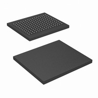
CY7C1412AV18-200BZC Cypress Semiconductor Corp, CY7C1412AV18-200BZC Datasheet - Page 4

CY7C1412AV18-200BZC
Manufacturer Part Number
CY7C1412AV18-200BZC
Description
SRAM (Static RAM)
Manufacturer
Cypress Semiconductor Corp
Datasheet
1.CY7C1412AV18-200BZXC.pdf
(27 pages)
Specifications of CY7C1412AV18-200BZC
Format - Memory
RAM
Memory Type
SRAM - Synchronous, QDR II
Memory Size
36M (2M x 18)
Speed
200MHz
Interface
Parallel
Voltage - Supply
1.7 V ~ 1.9 V
Operating Temperature
0°C ~ 70°C
Package / Case
165-TFBGA
Lead Free Status / RoHS Status
Contains lead / RoHS non-compliant
Available stocks
Company
Part Number
Manufacturer
Quantity
Price
Company:
Part Number:
CY7C1412AV18-200BZC
Manufacturer:
Cypress Semiconductor Corp
Quantity:
10 000
Pin Definitions
Document #: 38-05615 Rev. *H
D
WPS
BWS
BWS
BWS
BWS
A
Q
RPS
C
C
K
K
CQ
CQ
ZQ
DOFF
Pin Name
[x:0]
[x:0]
0
1
2
3
,
,
,
Input-
Synchronous
Input-
Synchronous
Input-
Synchronous
Input-
Synchronous
Outputs-
Synchronous
Input-
Synchronous
Input Clock
Input Clock
Input Clock
Input Clock
Echo Clock
Echo Clock
Input
Input
IO
Data Input Signals. Sampled on the rising edge of K and K clocks during valid write operations.
CY7C1412AV18 - D
CY7C1414AV18 - D
Write Port Select Active LOW. Sampled on the rising edge of the K clock. When asserted active, a
write operation is initiated. Deasserting deselects the write port. Deselecting the write port ignores D
Byte Write Select 0, 1, 2, and 3 Active LOW. Sampled on the rising edge of the K and K clocks during
write operations. Used to select which byte is written into the device during the current portion of the write
operations. Bytes not written remain unaltered.
CY7C1412AV18 BWS
CY7C1414AV18BWS
D
All the Byte Write Selects are sampled on the same edge as the data. Deselecting a Byte Write Select
ignores the corresponding byte of data and it is not written into the device.
Address Inputs. Sampled on the rising edge of the K (Read address) and K (Write address) clocks during
active read and write operations. These address inputs are multiplexed for both read and write operations.
Internally, the device is organized as 2M x 18 (2 arrays each of 1M x 18) for CY7C1412AV18 and 1M x
36 (2 arrays each of 512K x 36) for CY7C1414AV18. Therefore, only 20 address inputs are needed to
access the entire memory array of CY7C1412AV18 and 19 address inputs for CY7C1414AV18. These
inputs are ignored when the appropriate port is deselected.
Data Output Signals. These pins drive out the requested data during a read operation. Valid data is
driven out on the rising edge of both the C and C clocks during read operations, or K and K when in single
clock mode. When the read port is deselected, Q
CY7C1412AV18 Q
CY7C1414AV18 Q
Read Port Select Active LOW. Sampled on the rising edge of positive input clock (K). When active, a
read operation is initiated. Deasserting deselects the read port. When deselected, the pending access is
allowed to complete and the output drivers are automatically tri-stated following the next rising edge of
the C clock. Each read access consists of a burst of two sequential transfers.
Positive Input Clock for Output data. C is used in conjunction with C to clock out the read data from
the device. C and C can be used together to deskew the flight times of various devices on the board back
to the controller. See
Negative Input Clock for Output data. C is used in conjunction with C to clock out the read data from
the device. C and C can be used together to deskew the flight times of various devices on the board back
to the controller. See
Positive Input Clock Input. The rising edge of K is used to capture synchronous inputs to the device
and to drive out data through Q
edge of K.
Negative Input Clock Input. K is used to capture synchronous inputs being presented to the device and
to drive out data through Q
CQ Referenced with Respect to C. This is a free - running clock and is synchronized to the Input clock
for output data (C) of the QDR-II. In the single clock mode, CQ is generated with respect to K. The timings
for the echo clocks is shown in the
CQ Referenced with Respect to C. This is a free - running clock and is synchronized to the Input clock
for output data (C) of the QDR-II. In the single clock mode, CQ is generated with respect to K. The timings
for the echo clocks is shown in the
Output Impedance Matching Input. This input is used to tune the device outputs to the system data bus
impedance. CQ, CQ, and Q
between ZQ and ground. Alternatively, this pin can be connected directly to V
minimum impedance mode. This pin cannot be connected directly to GND or left unconnected.
DLL Turn Off Active LOW. Connecting this pin to ground turns off the DLL inside the device. The timing
in the DLL turned off operation differs from those listed in this data sheet.
[35:27].
[17:0]
[35:0]
[17:0]
[35:0]
Application Example
Application Example
0
0
controls D
controls D
[x:0]
[x:0]
when in single clock mode.
[x:0]
output impedance are set to 0.2 x RQ, where RQ is a resistor connected
[8:0]
Switching Characteristics
Switching Characteristics
when in single clock mode. All accesses are initiated on the rising
[8:0]
, BWS
, BWS
on page 7 for further details.
on page 7 for further details.
Pin Description
1
1
controls D
controls D
[x:0]
are automatically tri-stated.
[17:9]
[17:9]
,BWS
on page 21.
on page 21.
.
2
controls D
CY7C1412AV18
CY7C1414AV18
DDQ
[26:18]
, which enables the
and BWS
Page 4 of 27
3
controls
[x:0]
.
[+] Feedback


