EVAL-ADF7021-NDBEZ Analog Devices Inc, EVAL-ADF7021-NDBEZ Datasheet - Page 27
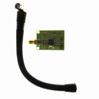
EVAL-ADF7021-NDBEZ
Manufacturer Part Number
EVAL-ADF7021-NDBEZ
Description
426MHz To 429 MHz, External L
Manufacturer
Analog Devices Inc
Type
Transceiver, FSKr
Datasheet
1.ADF7021-NBCPZ-RL.pdf
(64 pages)
Specifications of EVAL-ADF7021-NDBEZ
Frequency
420MHz ~ 440MHz
Lead Free Status / RoHS Status
Lead free / RoHS Compliant
For Use With/related Products
ADF7021-N
Lead Free Status / RoHS Status
Lead free / RoHS Compliant
Other names
Q5835434A


Setting the Transmit Data Rate
In all modulation modes except oversampled 2FSK mode, an
accurate clock is provided on the TxRxCLK pin to latch the data
from the microcontroller into the transmit section at the required
data rate. The exact frequency of this clock is defined by
where:
XTAL is the crystal or TCXO frequency.
DEMOD_CLK_DIVIDE is the divider that sets the demodulator
clock rate (R3_DB[6:9]).
CDR_CLK_DIVIDE is the divider that sets the CDR clock rate
(R3_DB[10:17]).
Refer to the Register 3—Transmit/Receive Clock Register
section for more programming information.
Setting the FSK Transmit Deviation Frequency
In all modulation modes, the deviation from the center
frequency is set using the Tx_FREQUENCY_DEVIATION bits
(R2_DB[19:27]).
The deviation from the center frequency in Hz is as follows:
For direct RF output,
For RF_DIVIDE_BY_2 enabled,
where Tx_FREQUENCY_DEVIATION is a number from 1 to
511 (R2_DB[19:27]).
In 4FSK modulation, the four symbols (00, 01, 11, 10) are
transmitted as ±3 × f
Binary Frequency Shift Keying (2FSK)
Two-level frequency shift keying is implemented by setting the
N value for the center frequency and then toggling it with the
TxDATA line. The deviation from the center frequency is set
using the Tx_FREQUENCY_DEVIATION bits, R2_DB[19:27].
2FSK is selected by setting the MODULATION_SCHEME bits
(R2_DB[4:6]) to 000.
Minimum shift keying (MSK) or Gaussian minimum shift
keying (GMSK) is supported by selecting 2FSK modulation and
using a modulation index of 0.5. A modulation index of 0.5 is
set up by configuring R2_DB[19:27] for an f
transmit data rate.
DATA
f
f
DEV
CLK
DEV
[
[
Hz
Hz
=
]
]
DEMOD
=
=
0
PFD
5 .
×
PFD
×
DEV
_
Tx
CLK
and ±1 × f
_
×
FREQUENCY
Tx
_
_
DIVIDE
FREQUENCY
2
16
DEV
XTAL
2
.
×
16
CDR
_
DEVIATION
_
_
DEV
DEVIATION
CLK
= 0.25 ×
_
DIVIDE
×
Rev. 0 | Page 27 of 64
32
3-Level Frequency Shift Keying (3FSK)
In 3-level FSK modulation (also known as modified duobinary
FSK), the binary data (Logic 0 and Logic 1) is mapped onto
three distinct frequencies: the carrier frequency (f
frequency minus a deviation frequency (f
carrier frequency plus the deviation frequency (f
A Logic 0 is mapped to the carrier frequency while a Logic 1 is
either mapped onto the f
frequency.
Compared to 2FSK, this bits-to-frequency mapping results in a
reduced transmission bandwidth because some energy is removed
from the RF sidebands and transferred to the carrier frequency.
At low modulation index, 3FSK improves the transmit spectral
efficiency by up to 25% when compared to 2FSK.
Bit-to-symbol mapping for 3FSK is implemented using a linear
convolutional encoder that also permits Viterbi detection to be
used in the receiver. A block diagram of the transmit hardware
used to realize this system is shown in Figure 43. The convolu-
tional encoder polynomial used to implement the transmit
spectral shaping is
where:
P is the convolutional encoder polynomial.
D is the unit delay operator.
A digital precoder with transfer function 1/P(D) implements an
inverse modulo-2 operation of the 1 − D
transmitter.
Tx DATA
0, 1
P(D) = 1 − D
PRECODER
1/P(D)
Figure 42. 3FSK Symbol-to-Frequency Mapping
2
f
C
0, 1
–
Figure 43. 3FSK Encoding
–1
f
DEV
RF FREQUENCY
C
− f
CONVOLUTIONAL
0, +1, –1
DATA FILTERING
DEV
f
0
C
ENCODER
CONTROL
FSK MOD
AND
P(D)
frequency or the f
f
C
+
+1
f
DEV
C
2
shaping filter in the
f
f
f
− f
C
C
C
+
–
DEV
f
f
DEV
DEV
ADF7021-N
C
), and the
C
), the carrier
+ f
C
+ f
DEV
TO
N DIVIDER
DEV
).
Related parts for EVAL-ADF7021-NDBEZ
Image
Part Number
Description
Manufacturer
Datasheet
Request
R

Part Number:
Description:
±1.7g Dual-Axis IMEMS Accelerometer Evaluation Board
Manufacturer:
Analog Devices Inc
Datasheet:

Part Number:
Description:
Inertial Sensor Evaluation System
Manufacturer:
Analog Devices Inc
Datasheet:
Part Number:
Description:
Manufacturer:
Analog Devices Inc
Datasheet:
Part Number:
Description:
Manufacturer:
Analog Devices Inc
Datasheet:
Part Number:
Description:
Manufacturer:
Analog Devices Inc
Datasheet:
Part Number:
Description:
Manufacturer:
Analog Devices Inc
Datasheet:
Part Number:
Description:
Manufacturer:
Analog Devices Inc
Datasheet:
Part Number:
Description:
Manufacturer:
Analog Devices Inc
Datasheet:
Part Number:
Description:
Manufacturer:
Analog Devices Inc
Datasheet:
Part Number:
Description:
Manufacturer:
Analog Devices Inc
Datasheet:
Part Number:
Description:
Manufacturer:
Analog Devices Inc
Datasheet:
Part Number:
Description:
Manufacturer:
Analog Devices Inc
Datasheet:
Part Number:
Description:
Manufacturer:
Analog Devices Inc
Datasheet: