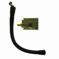
EVAL-ADF7021-NDBEZ Analog Devices Inc, EVAL-ADF7021-NDBEZ Datasheet - Page 29

EVAL-ADF7021-NDBEZ
Manufacturer Part Number
EVAL-ADF7021-NDBEZ
Description
426MHz To 429 MHz, External L
Manufacturer
Analog Devices Inc
Type
Transceiver, FSKr
Datasheet
1.ADF7021-NBCPZ-RL.pdf
(64 pages)
Specifications of EVAL-ADF7021-NDBEZ
Frequency
420MHz ~ 440MHz
Lead Free Status / RoHS Status
Lead free / RoHS Compliant
For Use With/related Products
ADF7021-N
Lead Free Status / RoHS Status
Lead free / RoHS Compliant
Other names
Q5835434A
2
3
1
Offset quadrature phase shift keying (OQPSK) with half sine baseband shaping
GMSK is GFSK with a modulation index = 0.5.
MSK is 2FSK modulation with a modulation index = 0.5.
MODULATION AND FILTERING OPTIONS
The various modulation and data filtering options are described
in Table 11.
Table 11. Modulation and Filtering Options
Modulation
BINARY FSK
3-LEVEL FSK
4-LEVEL FSK
is spectrally equivalent to MSK.
TRANSMIT LATENCY
Transmit latency is the delay time from the sampling of a
bit/symbol by the TxRxCLK signal to when that bit/symbol
appears at the RF output. The latency without any data filtering
is one bit. The addition of data filtering adds a further latency as
outlined in Table 12.
It is important that the ADF7021-N be left in transmit mode
after the last data bit is sampled by the data clock to account for
this latency. The ADF7021-N should stay in transmit mode for
a time equal to the number of latency bit periods for the applied
modulation scheme. This ensures that all of the data sampled by
the TxRxCLK signal appears at RF.
The figures for latency in Table 12 assume that the positive
TxRxCLK edge is used to sample data (default). If the TxRxCLK
is inverted by setting R2_DB[28:29], an additional 0.5 bit
latency can be added to all values in Table 12.
OQPSK with Half Sine
Baseband Shaping
2FSK
MSK
GFSK
GMSK
RC2FSK
Oversampled 2FSK
3FSK
RC3FSK
4FSK
RC4FSK
1
3
2
Data Filtering
None
None
None
Gaussian
Gaussian
Raised cosine
None
None
Raised cosine
None
Raised cosine
R2_DB[4:6]
000
000
000
001
001
101
100
010
110
011
111
Rev. 0 | Page 29 of 64
Table 12. Bit/Symbol Latency in Transmit Mode for Various
Modulation Schemes
Modulation
2FSK
3FSK
4FSK
TEST PATTERN GENERATOR
The ADF7021-N has a number of built-in test pattern generators
that can be used to facilitate radio link setup or RF measurement.
A full list of the supported patterns is shown in Table 13. The
data rate for these test patterns is the programmed data rate set
in Register 3.
The PN9 sequence is suitable for test modulation when carrying
out adjacent channel power (ACP) or occupied bandwidth
measurements.
Table 13. Transmit Test Pattern Generator Options
Test Pattern
Normal
Transmit Carrier
Transmit + f
Transmit − f
Transmit 1010 Pattern
Transmit PN9 Sequence
Transmit SWD Pattern Repeatedly
GFSK
RC2FSK, Alpha = 0.5
RC2FSK, Alpha = 0.7
RC3FSK, Alpha = 0.5
RC3FSK, Alpha = 0.7
RC4FSK, Alpha = 0.5
RC4FSK, Alpha = 0.7
DEV
DEV
Tone
Tone
Latency
1 bit
4 bits
5 bits
4 bits
1 bit
5 bits
4 bits
1 symbol
5 symbols
4 symbols
R15_DB[8:10]
000
001
010
011
100
101
110
ADF7021-N


