EVAL-ADF7021-NDBEZ Analog Devices Inc, EVAL-ADF7021-NDBEZ Datasheet - Page 46
EVAL-ADF7021-NDBEZ
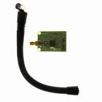
Manufacturer Part Number
EVAL-ADF7021-NDBEZ
Description
426MHz To 429 MHz, External L
Manufacturer
Analog Devices Inc
Type
Transceiver, FSKr
Datasheet
1.ADF7021-NBCPZ-RL.pdf
(64 pages)
Specifications of EVAL-ADF7021-NDBEZ
Frequency
420MHz ~ 440MHz
Lead Free Status / RoHS Status
Lead free / RoHS Compliant
For Use With/related Products
ADF7021-N
Lead Free Status / RoHS Status
Lead free / RoHS Compliant
Other names
Q5835434A


ADF7021-N
SERIAL INTERFACE
The serial interface allows the user to program the 16-/32-bit
registers using a 3-wire interface (SCLK, SDATA, and SLE).
It consists of a level shifter, 32-bit shift register, and 16 latches.
Signals should be CMOS compatible. The serial interface is
powered by the regulator, and, therefore, is inactive when CE is low.
Data is clocked into the register, MSB first, on the rising edge of
each clock (SCLK). Data is transferred to one of 16 latches on the
rising edge of SLE. The destination latch is determined by the
value of the four control bits (C4 to C1); these are the bottom
4 LSBs, DB3 to DB0, as shown in Figure 2. Data can also be read
back on the SREAD pin.
READBACK FORMAT
The readback operation is initiated by writing a valid control
word to the readback register and enabling the READBACK bit
(R7_DB8 = 1). The readback can begin after the control word
has been latched with the SLE signal. SLE must be kept high
while the data is being read out. Each active edge at the SCLK
pin successively clocks the readback word out at the SREAD
pin, as shown in Figure 58, starting with the MSB first. The data
appearing at the first clock cycle following the latch operation
must be ignored. An extra clock cycle is needed after the 16
readback bit to return the SREAD pin to tristate. Therefore, 18
total clock cycles are needed for each read back. After the 18
clock cycle, SLE should be brought low.
BATTERY VOLTAGE/ADCIN/
TEMP. SENSOR READBACK
FILTER CAL READBACK
READBACK MODE
SILICON REVISION
RSSI READBACK
AFC READBACK
DB15
RV16
RV16
X
X
0
DB14
RV15
RV15
X
X
0
DB13
RV14
RV14
X
X
0
DB12
RV13
RV13
X
X
0
Figure 58. Readback Value Table
DB11
RV12
RV12
X
X
0
th
th
Rev. 0 | Page 46 of 64
DB10
RV11
RV11
LG2
X
0
RV10
RV10
DB9
LG1
X
0
READBACK VALUE
AFC Readback
The AFC readback is valid only during the reception of FSK
signals with either the linear or correlator demodulator active.
The AFC readback value is formatted as a signed 16-bit integer
comprising Bit RV1 to Bit RV16 and is scaled according to the
following formula:
In the absence of frequency errors, FREQ RB is equal to the IF
frequency of 100 kHz. Note that, for the AFC readback to yield
a valid result, the downconverted input signal must not fall outside
the bandwidth of the analog IF filter. At low input signal levels,
the variation in the readback value can be improved by averaging.
RSSI Readback
The format of the readback word is shown in Figure 58. It
comprises the RSSI-level information (Bit RV1 to Bit RV7), the
current filter gain (FG1, FG2), and the current LNA gain (LG1,
LG2) setting. The filter and LNA gain are coded in accordance
with the definitions in the Register 9—AGC Register section. For
signal levels below −100 dBm, averaging the measured RSSI values
improves accuracy. The input power can be calculated from the
RSSI readback value as outlined in the RSSI/AGC section.
DB8
RV9
FG2
RV9
X
0
FREQ RB [Hz] = (AFC_READBACK × DEMOD CLK)/2
DB7
RV8
FG1
RV8
RV8
X
DB6
RV7
RV7
RV7
RV7
RV7
DB5
RV6
RV6
RV6
RV6
RV6
DB4
RV5
RV5
RV5
RV5
RV5
DB3
RV4
RV4
RV4
RV4
RV4
DB2
RV3
RV3
RV3
RV3
RV3
DB1
RV2
RV2
RV2
RV2
RV2
DB0
RV1
RV1
RV1
RV1
RV1
18
Related parts for EVAL-ADF7021-NDBEZ
Image
Part Number
Description
Manufacturer
Datasheet
Request
R

Part Number:
Description:
±1.7g Dual-Axis IMEMS Accelerometer Evaluation Board
Manufacturer:
Analog Devices Inc
Datasheet:

Part Number:
Description:
Inertial Sensor Evaluation System
Manufacturer:
Analog Devices Inc
Datasheet:
Part Number:
Description:
Manufacturer:
Analog Devices Inc
Datasheet:
Part Number:
Description:
Manufacturer:
Analog Devices Inc
Datasheet:
Part Number:
Description:
Manufacturer:
Analog Devices Inc
Datasheet:
Part Number:
Description:
Manufacturer:
Analog Devices Inc
Datasheet:
Part Number:
Description:
Manufacturer:
Analog Devices Inc
Datasheet:
Part Number:
Description:
Manufacturer:
Analog Devices Inc
Datasheet:
Part Number:
Description:
Manufacturer:
Analog Devices Inc
Datasheet:
Part Number:
Description:
Manufacturer:
Analog Devices Inc
Datasheet:
Part Number:
Description:
Manufacturer:
Analog Devices Inc
Datasheet:
Part Number:
Description:
Manufacturer:
Analog Devices Inc
Datasheet:
Part Number:
Description:
Manufacturer:
Analog Devices Inc
Datasheet: