JN5139-001-M/04R1T NXP Semiconductors, JN5139-001-M/04R1T Datasheet - Page 2
JN5139-001-M/04R1T
Manufacturer Part Number
JN5139-001-M/04R1T
Description
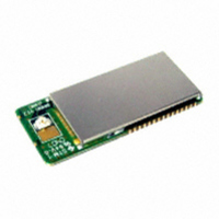
JN5139-001-M/SOM041/REEL13 DP
Manufacturer
NXP Semiconductors
Series
JN5139-001-M0xRr
Specifications of JN5139-001-M/04R1T
Frequency
2.4GHz
Modulation Or Protocol
802.15.4 Zigbee
Applications
Home/Building Automation, Industrial Control and Monitoring
Power - Output
19dBm
Sensitivity
-97dBm
Voltage - Supply
2.7 V ~ 3.6 V
Current - Receiving
45mA
Current - Transmitting
120mA
Data Interface
PCB, Surface Mount
Memory Size
96kB RAM, 192kB ROM
Antenna Connector
PCB, Surface Mount
Operating Temperature
-20°C ~ 70°C
Package / Case
Module
Core
RISC
Interface Type
SPI, UART
Core Architecture
RISC
Lead Free Status / RoHS Status
Lead free / RoHS Compliant
Data Rate - Maximum
-
Lead Free Status / Rohs Status
Details
Other names
616-1041-2
935294017534
JN5139-001-M04
JN5139-001-M04R1T
JN5139-001-M04R1T
Q3424158
935294017534
JN5139-001-M04
JN5139-001-M04R1T
JN5139-001-M04R1T
Q3424158
Available stocks
Company
Part Number
Manufacturer
Quantity
Price
Company:

Part Number:
JN5139-001-M/04R1T
Manufacturer:
VTTESSE
Quantity:
156


Contents
1. Introduction
1.1.
1.2.
2. Specifications
3. Product Development
3.1.
4. Pin Configurations
4.1.
4.2.
4.2.1
4.2.2
5. Electrical Characteristics
5.1.
5.2.
5.3.
Appendix A Additional Information
A.1 Outline Drawing
A.2 Module PCB Footprint
A.3 Ordering Information
A.4 Tape and Reel Information:
A.4.1
A.4.2 Cover tape details
A.4.3 Leader and Trailer
A.4.4 Reel Dimensions:
A.5 Related Documents
A.6 Federal Communication Commission Interference Statement
A.6.1 Antennas approved by FCC for use with JN5139 modules
A.6.2 High Power Module usage limitation
A.6.3 FCC End Product Labelling
A.7 European R & TTE Directive 1999/5/EC Statement
A.8 Industry Canada Statement
A.8.1 Industry Canada End Product Labelling
A.9 RoHS Compliance
A.10 Status Information
A.11 Disclaimers
A.12 Version Control
ii
Tape Orientation and dimensions
Variants
Regulatory Approvals
JN5139 Single Chip Wireless Microcontroller
Pin Assignment
Pin Descriptions
Maximum Ratings
Reflow Profile
Operating Conditions
Power Supplies
SPI Memory Connections
JN-DS-JN5139-xxx-Myy 1v6
© NXP Laboratories UK 2010
10
11
11
16
17
18
18
18
19
19
20
20
21
22
22
23
24
24
24
25
25
26
3
4
5
6
9
3
3
5
7
8
8
8
9
9
Related parts for JN5139-001-M/04R1T
Image
Part Number
Description
Manufacturer
Datasheet
Request
R

Part Number:
Description:
JN5139-001-M/SOM041/REEL PACK/
Manufacturer:
NXP Semiconductors
Datasheet:

Part Number:
Description:
JN5139-001-M/SOM041/REEL13 DP
Manufacturer:
NXP Semiconductors
Datasheet:

Part Number:
Description:
JN5139-001-M/SOM041/REEL PACK/
Manufacturer:
NXP Semiconductors
Datasheet:

Part Number:
Description:
JN5139-001-M/SOM041/REEL13 DP
Manufacturer:
NXP Semiconductors
Datasheet:
Part Number:
Description:
IC MCU 802.15.4 32BIT 2.4G 56QFN
Manufacturer:
NXP Semiconductors
Datasheet:

Part Number:
Description:
MCU 802.15.4 32BIT 2.4G 56-QFN
Manufacturer:
NXP Semiconductors
Datasheet:

Part Number:
Description:
IC MCU 32BIT 56QFN
Manufacturer:
NXP Semiconductors
Datasheet:
Part Number:
Description:
MCU 802.15.4 32BIT 2.4G 56-QFN
Manufacturer:
NXP Semiconductors
Datasheet:
Part Number:
Description:
NXP Semiconductors designed the LPC2420/2460 microcontroller around a 16-bit/32-bitARM7TDMI-S CPU core with real-time debug interfaces that include both JTAG andembedded trace
Manufacturer:
NXP Semiconductors
Datasheet:

Part Number:
Description:
NXP Semiconductors designed the LPC2458 microcontroller around a 16-bit/32-bitARM7TDMI-S CPU core with real-time debug interfaces that include both JTAG andembedded trace
Manufacturer:
NXP Semiconductors
Datasheet:
Part Number:
Description:
NXP Semiconductors designed the LPC2468 microcontroller around a 16-bit/32-bitARM7TDMI-S CPU core with real-time debug interfaces that include both JTAG andembedded trace
Manufacturer:
NXP Semiconductors
Datasheet:
Part Number:
Description:
NXP Semiconductors designed the LPC2470 microcontroller, powered by theARM7TDMI-S core, to be a highly integrated microcontroller for a wide range ofapplications that require advanced communications and high quality graphic displays
Manufacturer:
NXP Semiconductors
Datasheet:
Part Number:
Description:
NXP Semiconductors designed the LPC2478 microcontroller, powered by theARM7TDMI-S core, to be a highly integrated microcontroller for a wide range ofapplications that require advanced communications and high quality graphic displays
Manufacturer:
NXP Semiconductors
Datasheet:
Part Number:
Description:
The Philips Semiconductors XA (eXtended Architecture) family of 16-bit single-chip microcontrollers is powerful enough to easily handle the requirements of high performance embedded applications, yet inexpensive enough to compete in the market for hi
Manufacturer:
NXP Semiconductors
Datasheet: