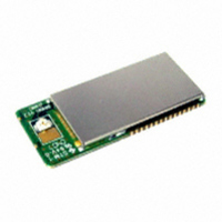
JN5139-001-M/04R1T NXP Semiconductors, JN5139-001-M/04R1T Datasheet - Page 9

JN5139-001-M/04R1T
Manufacturer Part Number
JN5139-001-M/04R1T
Description
JN5139-001-M/SOM041/REEL13 DP
Manufacturer
NXP Semiconductors
Series
JN5139-001-M0xRr
Specifications of JN5139-001-M/04R1T
Frequency
2.4GHz
Modulation Or Protocol
802.15.4 Zigbee
Applications
Home/Building Automation, Industrial Control and Monitoring
Power - Output
19dBm
Sensitivity
-97dBm
Voltage - Supply
2.7 V ~ 3.6 V
Current - Receiving
45mA
Current - Transmitting
120mA
Data Interface
PCB, Surface Mount
Memory Size
96kB RAM, 192kB ROM
Antenna Connector
PCB, Surface Mount
Operating Temperature
-20°C ~ 70°C
Package / Case
Module
Core
RISC
Interface Type
SPI, UART
Core Architecture
RISC
Lead Free Status / RoHS Status
Lead free / RoHS Compliant
Data Rate - Maximum
-
Lead Free Status / Rohs Status
Details
Other names
616-1041-2
935294017534
JN5139-001-M04
JN5139-001-M04R1T
JN5139-001-M04R1T
Q3424158
935294017534
JN5139-001-M04
JN5139-001-M04R1T
JN5139-001-M04R1T
Q3424158
Available stocks
Company
Part Number
Manufacturer
Quantity
Price
Company:
Part Number:
JN5139-001-M/04R1T
Manufacturer:
VTTESSE
Quantity:
156
5. Electrical Characteristics
In most cases, the Electrical Characteristics are the same for both module and chip. They are described in detail in
the chip datasheet. Where there are differences, they are detailed below.
5.1. Maximum Ratings
Exceeding these conditions will result in damage to the device.
This device is sensitive to ESD and should only be handled using ESD precautions.
5.2. Reflow Profile
For reflow soldering, it is recommended to follow the reflow profile in Figure 2 as a guide, as well as the paste
manufacturers guidelines on peak flow temperature, soak times, time above liquidus and ramp rates.
© NXP Laboratories UK 2010
Temperature
Target Time (s)
Device supply voltage VDD
Voltage on analogue pins: ADC1-4, DAC1-2, COMP1-,
COMP1+, COMP2-, COMP2+, DIO9, DIO10, SPISSM,
SPISWP, SPICLK, SPIMOSI, SPIMISO,
Voltage on 5v tolerant digital pins: SPISSZ, DIO0-
DIO8, DIO11-DIO20, RESETN
Storage temperature
Reflow soldering temperature according to IPC/JEDEC
J-STD-020C
Parameter
25~160 ºC
90~130
Figure 2: Recommended solder reflow profile
JN-DS-JN5139-xxx-Myy 1v6
160~190 ºC
30~60
> 220º C
20~50
-40ºC
-0.3V
-0.3V
-0.3V
Min
230~Pk.
10~15
Lower of (VDD + 2V)
VDD + 0.3V
and 5.5V
150ºC
260ºC
3.6V
Max
Pk. Temp
160~270
(235ºC)
9


