ADNS-2220 Avago Technologies US Inc., ADNS-2220 Datasheet
ADNS-2220
Specifications of ADNS-2220


Related parts for ADNS-2220


ADNS-2220 Summary of contents
Page 1
... The ADNS-3060 along with the ADNS-2120 (or ADNS-2120- 001) lens, ADNS-2220 (or ADNS-2220-001) assembly clip and HLMP-ED80-XX000 form a complete, compact optical mouse tracking system. There are no moving parts, which means high reliability and less maintenance for the end user. In ad- dition, precision optical alignment is not required, facilitating high volume assembly ...
Page 2
Pinout Pin Name Description 1 NCS Chip select (active low input) 2 MISO Serial data output (Master In/Slave Out) 3 SCLK Serial clock input 4 MOSI Serial data input (Master Out/Slave In) 5 LED_CTRL LED control output 6 RESET Reset ...
Page 3
Figure 2. Package outline drawing CAUTION advised that normal static precautions be taken in handling and assembly of this component to prevent damage and/or degradation which may be induced by ESD. 3 ...
Page 4
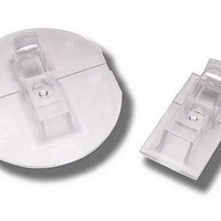
... ESD events that occur at the opening of the base plate. The ADNS-2220-001 clip holds the LED in relation to the lens. The LED must be inserted into the clip and the LED’s leads formed prior to loading on the PCB. The clip interlocks the sensor to the lens, and through the lens to the alignment features on the base plate ...
Page 5
... NOTE: These new Avago Technologies optical mouse sensors, lenses and clips have different physical configura- tions that require a different PCB mounting method to optimize the navigation performance. Refer Application Notes AN 5035 : ADNS-3060 PCB Mounting Method for ADNS-3060 Optical Sensor for further information. ...
Page 6
... PROCESSOR MISO LED_CTRL CTRL RESET Figure 6. Block diagram of ADNS-3060 optical mouse sensor 6 HLMP-ED80-XX000 (LED) ADNS-2220 (Clip) ADNS-3060 (Sensor) Customer supplied PCB ADNS-2120 (Lens) Customer supplied base plate with recommended alignment features per IGES drawing. 6. Remove the protective kapton tape from optical aperture of the sensor ...
Page 7
... The table below shows typical values assum- ing base plate construction per the Avago Technologies supplied IGES file and ADNS-2120 lens flange. For improved ESD performance, the lens flange can be sealed (i.e. glued) to the base plate. Note that the lens ...
Page 8
... NC pins should not be connected to any traces. x Surface mount parts are recommended. x Care must be taken when interfacing a 5V microcontroller to the ADNS-3060. Serial port inputs on the sensor should be connected to open- drain outputs from the microcontroller or use an active drive level shifter. NPD and RESET should be connected to 5V microcontroller outputs through a resistor divider or other level shifting technique ...
Page 9
... The external program is supplied by Avago Technologies as a file which may be burned into a programmable device. A micro-controller with sufficient memory may be used. On power-up and reset, the ADNS- 3060 program is downloaded into volatile memory using the burst-mode procedure described in the Synchronous Serial Port section. The program size is 1986 x 8 bits. ...
Page 10
Absolute Maximum Ratings Parameter Symbol Storage Temperature T S Operating Temperature T A Lead Solder Temp Supply Voltage V DD3 ESD Input Voltage V IN Output current I out Recommended Operating Conditions Parameter Symbol Operating Temperature T A Power supply ...
Page 11
AC Electrical Specifications Electrical Characteristics over recommended operating conditions. Typical values at 25 °C, V Parameter Symbol Minimum Typical VDD to RESET t OP Data delay after t PU-RESET RESET Input delay after T IN-RST reset Power Down t PD ...
Page 12
DC Electrical Specifications Electrical Characteristics over recommended operating conditions. Typical values at 25 °C, V Parameter Symbol Minimum DC Supply Current I DD_AVG Power Down I DDPD Supply Current Input Low Voltage V IL Input High Voltage V 0.7 * ...
Page 13
Typical Performance Characteristics Typical Resolution vs. Z-heights 1000 900 800 700 600 DOF 500 400 300 200 Recommended 100 Operating Region 0 -100 Z-heights - mm (2.4 = Nominal Focus) Figure 11. Mean Resolution vs. Z (White Paper) Typical Path ...
Page 14
... Figure 14. Idd vs. Frame Rate Synchronous Serial Port The synchronous serial port is used to set and read pa- rameters in the ADNS-3060, and to read out the motion information. The serial port is also used to load SROM data into the ADNS-3060. The port is a four-wire, serial port. The host micro-con- troller always initiates communication ...
Page 15
... The 250 ns minimum high state of SCLK is also the mini- mum MISO data hold time of the ADNS-3060. Since the falling edge of SCLK is actually the start of the next read or write command, the ADNS-3060 will hold the state of data on MISO until the falling edge of SCLK. SCLK ...
Page 16
... The falling edge of SCLK for the first address bit of either the read or write command must be at least 250 ns after the last SCLK rising edge of the last data bit of the previous read operation. In addition, during a read operation SCLK should be delayed after the last address bit to ensure that the ADNS-3060 has time to prepare the requested data. 16 ≥ ...
Page 17
... Figure 22. Motion burst timing 17 Motion Read This mode is activated by reading the Motion_Burst register. The ADNS-3060 will respond with the contents of the Motion, Delta_X, Delta_Y, SQUAL, Shutter_Upper, Shutter_Lower and Maximum_Pixel registers in that order. After sending the register address, the micro- controller must wait t data ...
Page 18
... SROM Download This function is used to load the Avago Technologies supplied firmware file contents into the ADNS-3060. The firmware fi ASCII text file with each 2-character byte (hexadecimal representation single line. This mode is activated by the following steps: 1. Perform hardware reset by toggling the RESET pin 2 ...
Page 19
Frame Capture This is a fast way to download a full array of pixel values from a single frame. This mode disables navigation and overwrites any downloaded firmware. A hardware reset is required to restore navigation, and the firmware must ...
Page 20
... ESD events, power sup- ply droops or micro-controller firmware flaws. In such a case, the micro-controller should pulse NCS high for at least 1 ms. The ADNS-3060 will reset the serial port (but not the control registers) and will be prepared for the beginning of a new transmission after the normal transaction delay ...
Page 21
... Notes on Power-up and the serial port Reset Circuit The ADNS-3060 does not perform an internal power up self-reset. The reset pin must be raised and lowered to reset the chip. This should be done every time power is applied. During power-up there will be a period of time after the power supply is high but before any clocks are available ...
Page 22
... Registers The ADNS-3060 registers are accessible via the serial port. The registers are used to read motion data and status as well as to set the device configuration. Address Register 0x00 Product_ID 0x01 Revision_ID 0x02 Motion 0x03 Delta_X 0x04 Delta_Y 0x05 SQUAL 0x06 ...
Page 23
... Field PID PID 7 6 Data Type: 8-Bit unsigned integer USAGE: This register contains a unique identification assigned to the ADNS-3060. The value in this register does not change; it can be used to verify that the serial communications link is functional. Revision_ID Access: Read Bit 7 6 Field ...
Page 24
Notes for Motion: 1. Reading this register freezes the Delta_X and Delta_Y register values. Read this register before reading the Delta_X and Delta_Y registers. If Delta_X and Delta_Y are not read before the motion register is read a second time, ...
Page 25
SQUAL Access: Read Bit 7 6 Field Data Type: Upper 8 bits of a 10-bit unsigned integer. USAGE: SQUAL (Surface Quality measure of ¼ of the number of valid* features visible by the sensor ...
Page 26
Pixel_Sum Access: Read Bit 7 6 Field Data Type: High 8 bits of an unsigned 16-bit integer. USAGE: This register is used to find the average pixel value. It reports the upper byte of a 16-bit ...
Page 27
Configuration_bits Access: Read/Write Bit 7 6 Field 0 LED_MODE Data Type: Bit field USAGE: Register 0x0a allows the user to change the configuration of the sensor. Shown below are the bits, their default values, and optional values. Field Name Description ...
Page 28
Extended_Config Access: Read/Write Bit 7 6 Field Busy Reserved Data Type: Bit field USAGE: Register 0x0b allows the user to change the configuration of the sensor. Shown below are the bits, their default values, and optional values. Field Name Description ...
Page 29
Data_Out_Lower Access: Read Bit 7 6 Field Data_Out_Upper Access: Read Bit 7 6 Field Data Type: Sixteen bit word. USAGE: Data in these registers come from the system self test or the ...
Page 30
Shutter_Lower Access: Read Bit 7 6 Field Shutter_Upper Access: Read Bit 7 6 Field Data Type: Sixteen bit unsigned integer. USAGE: Units are clock cycles. Read Shutter_Upper first, then Shutter_Lower. They should ...
Page 31
Frame_Period_Lower Access: Read Bit 7 6 Field Frame_Period_Upper Access: Read Bit 7 6 Field Data Type: Sixteen bit unsigned integer. USAGE: Read these registers to determine the current frame period and to ...
Page 32
Frame_Capture Access: Read/Write Bit 7 6 Field Data Type: Bit field USAGE: Writing 0x83 to this register will cause the next available complete 1 2/3 frames of pixel values to be stored to SROM RAM. Writing ...
Page 33
Frame_Period_Max_Bound_Lower Access: Read/Write Bit 7 6 Field FBm FBm 7 6 Frame_Period_Max_Bound_Upper Access: Read/Write Bit 7 6 Field FBm FBm 15 14 Data Type: 16-bit unsigned integer. USAGE: This value sets the maximum frame period (the MINIMUM frame rate) which ...
Page 34
Frame_Period_Min_Bound_Lower Access: Read/Write Bit 7 6 Field FBm FBm 7 6 Frame_Period_Min_Bound_Upper Access: Read/Write Bit 7 6 Field FBm FBm 15 14 Data Type: 16-bit unsigned integer. USAGE: This value sets the minimum frame period (the MAXIMUM frame rate) that ...
Page 35
Shutter_Max_Bound_Lower Access: Read/Write Bit 7 6 Field Shutter_Max_Bound_Upper Access: Read/Write Bit 7 6 Field Data Type: 16-bit unsigned integer. USAGE: This value sets the maximum allowable shutter value when operating in automatic ...
Page 36
Reserved Observation Access: Read/Write Bit 7 6 Field OB Reserved 7 Data Type: Bit field USAGE: Each bit is set by some process or action at regular intervals, or when the event occurs. The user must clear the register by ...
Page 37
... Upper, and Shutter_Lower and Maximum_Pixel registers. See the Synchronous Serial Port section for use details. SROM_Load Access: Write Data Type: Eight bit unsigned integer USAGE: The SROM_Load register is used for high-speed programming of the ADNS-3060 from an external SROM or microcontroller. See the Synchronous Serial Port section for use details. 37 Address: 0x40 ...
Page 38
... ADNS-3060 = Sensor pin plastic optical package, 20 per tube. ADNS-2120 = Round Optical Mouse Lens ADNS-2120-001 = Trim Optical Mouse Lens ADNS-2220 = LED Assembly Clip (Clear) ADNS-2220-001 LED Assembly Clip (Black) HLMP-ED80-XX000 = LED For product information and a complete list of distributors, please go to our web site: Avago, Avago Technologies, and the A logo are trademarks of Avago Technologies in the United States and other countries. Data subject to change. Copyright © ...