MRF8P8300HR6 Freescale Semiconductor, MRF8P8300HR6 Datasheet
MRF8P8300HR6
Specifications of MRF8P8300HR6


Related parts for MRF8P8300HR6

MRF8P8300HR6 Summary of contents
Page 1
... SINGLE W- -CDMA LATERAL N- -CHANNEL RF POWER MOSFETs CASE 375D- -05, STYLE 1 NI- -1230 MRF8P8300HR6 CASE 375E- -04, STYLE 1 NI- -1230S MRF8P8300HSR6 inA GSA inB GSB (Top View) Figure 1. Pin Connections (2,3) Symbol Value R θJC 0.26 0.21 MRF8P8300HR6 MRF8P8300HSR6 /V outA DSA /V outB DSB Unit °C/W 1 ...
Page 2
... Single--Carrier W--CDMA, IQ Magnitude Clipping, Input Signal PAR = 7 0.01% Probability on CCDF. ACPR measured in 3.84 MHz Channel Bandwidth @ ±5 MHz Offset. Frequency 790 MHz 805 MHz 820 MHz 1. Each side of device measured separately. 2. Part internally matched both on input and output. MRF8P8300HR6 MRF8P8300HSR6 2 = 25°C unless otherwise noted) Symbol I DSS I DSS ...
Page 3
... IMD sym VBW res = 96 W Avg. G out F ∆G ∆P1dB Min Typ Max = 2000 mA, 790--820 MHz Bandwidth — 340 — — 35 — — 35 — — 0.5 — — 0.0185 — — 0.0076 — MRF8P8300HR6 MRF8P8300HSR6 Unit W MHz MHz dB dB/°C dB/°C 3 ...
Page 4
... C6* C24 *C5, C6, C47, and C48 are mounted vertically. Figure 2. MRF8P8300HR6(HSR6) Test Circuit Component Layout Table 5. MRF8P8300HR6(HSR6) Test Circuit Component Designations and Values Part B1, B2 Short Ferrite Beads C1, C2, C39, C40, C41, C42 2.1 pF Chip Capacitors C3, C49, C50 1.0 pF Chip Capacitors C4 120 pF Chip Capacitor ...
Page 5
... RF Device Data Freescale Semiconductor Devices are tested in a parallel configuration Single--ended λ λ Quadrature combined 4 4 λ λ λ λ Doherty 4 4 λ λ λ λ Push--pull Possible Circuit Topologies Figure 3. MRF8P8300HR6 MRF8P8300HSR6 5 ...
Page 6
... MRF8P8300HR6 MRF8P8300HSR6 6 TYPICAL CHARACTERISTICS η Vdc (Avg.), I = 2000 mA DD out DQ Single--Carrier W--CDMA, 3.84 MHz Channel Bandwidth Input Signal PAR = 7 0.01% Probability on CCDF PARC IRL ACPR 750 770 790 810 830 850 f, FREQUENCY (MHz Watts Avg ...
Page 7
... MHz --70 -- --90 --100 --9 Figure 10. Single- -Carrier W- -CDMA Spectrum 66 0 790 MHz --10 55 η --20 ACPR -- --50 0 --60 400 --5 --10 --15 --20 1000 1060 3.84 MHz Channel BW +ACPR in 3.84 MHz Integrated BW Integrated BW --7.2 --5.4 --3.6 --1.8 0 1.8 3.6 5.4 f, FREQUENCY (MHz) MRF8P8300HR6 MRF8P8300HSR6 7 ...
Page 8
... Figure 11. Series Equivalent Source and Load Impedance MRF8P8300HR6 MRF8P8300HSR6 Vdc 2000 mA Avg out source load MHz Ω Ω 730 1.07 -- j1.15 0.86 -- j0.18 750 1.06 -- j0.97 0.90 + j0.04 770 1.11 -- j0.78 1.07 + j0.46 790 1.05 -- j0.62 1.28 -- j0.67 810 1.11 -- j0.45 ...
Page 9
... P1dB 1.16 -- j1.39 822 P1dB 1.24 -- j1.73 Figure 12. Pulsed CW Output Power versus Input Power @ 28 V Ideal Actual 822 MHz 806 MHz 790 MHz 40 41.5 P3dB dBm 55.6 55.6 55.4 Z load Ω 0.78 -- j0.73 0.76 -- j0.71 0.76 -- j0.74 MRF8P8300HR6 MRF8P8300HSR6 9 ...
Page 10
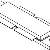
... MRF8P8300HR6 MRF8P8300HSR6 10 PACKAGE DIMENSIONS RF Device Data Freescale Semiconductor ...
Page 11
... RF Device Data Freescale Semiconductor MRF8P8300HR6 MRF8P8300HSR6 11 ...
Page 12
... MRF8P8300HR6 MRF8P8300HSR6 12 RF Device Data Freescale Semiconductor ...
Page 13
... RF Device Data Freescale Semiconductor MRF8P8300HR6 MRF8P8300HSR6 13 ...
Page 14
... MRF8P8300H and MRF8P8300HS in the R6 tape and reel option. The following table summarizes revisions to this document. Revision Date 0 Jan. 2011 • Initial Release of Data Sheet MRF8P8300HR6 MRF8P8300HSR6 14 R5 TAPE AND REEL OPTION REVISION HISTORY Description RF Device Data Freescale Semiconductor ...
Page 15
... Freescale Semiconductor was negligent regarding the design or manufacture of the part. Freescalet and the Freescale logo are trademarks of Freescale Semiconductor, Inc. All other product or service names are the property of their respective owners. © Freescale Semiconductor, Inc. 2011. All rights reserved. MRF8P8300HR6 MRF8P8300HSR6 15 ...