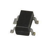
BFG67 T/R NXP Semiconductors, BFG67 T/R Datasheet - Page 6

BFG67 T/R
Manufacturer Part Number
BFG67 T/R
Description
RF Bipolar Small Signal TAPE7 TNS-RFSS
Manufacturer
NXP Semiconductors
Datasheet
1.BFG67_TR.pdf
(14 pages)
Specifications of BFG67 T/R
Dc Collector/base Gain Hfe Min
60
Mounting Style
SMD/SMT
Configuration
Single
Transistor Polarity
NPN
Maximum Operating Frequency
8000 MHz
Collector- Emitter Voltage Vceo Max
10 V
Emitter- Base Voltage Vebo
2.5 V
Continuous Collector Current
0.05 A
Power Dissipation
380 mW
Maximum Operating Temperature
+ 175 C
Package / Case
SOT-143
Lead Free Status / RoHS Status
Lead free / RoHS Compliant
Other names
BFG67,215
NXP Semiconductors
handbook, halfpage
handbook, halfpage
NPN 8 GHz wideband transistors
V
G
MSG = maximum stable gain;
G
V
G
MSG = maximum stable gain;
G
CE
CE
UM
max
UM
max
gain
(dB)
gain
(dB)
= 8 V; I
= 8 V; I
50
50
40
30
20
10
40
30
20
10
= maximum unilateral power gain;
= maximum unilateral power gain;
= maximum available gain.
= maximum available gain.
0
0
10
10
Fig.10 Gain as a function of frequency.
Fig.8 Gain as a function of frequency.
C
C
= 5 mA.
= 30 mA.
10
10
MSG
2
2
G UM
MSG
G UM
10
10
3
3
G max
f (MHz)
f (MHz)
G max
MBB305
MBB307
10
10
Rev. 05 - 23 November 2007
4
4
handbook, halfpage
handbook, halfpage
V
G
MSG = maximum stable gain;
G
V
CE
CE
(dB)
UM
max
gain
(dB)
Fig.11 Minimum noise figure as a function of
F
= 8 V; I
= 8 V.
50
= maximum unilateral power gain;
40
30
20
10
= maximum available gain.
4
3
2
0
0
1
10
1
Fig.9 Gain as a function of frequency.
BFG67; BFG67/X; BFG67/XR
C
= 15 mA.
collector current.
10
2
MSG
G UM
10
10
I
C
3
Product specification
(mA)
f (MHz)
900 MHz
500 MHz
f = 2 GHz
1 GHz
G max
MBB308
MBB306
6 of 14
100
10
4


