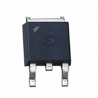
FDD3672 Fairchild Semiconductor, FDD3672 Datasheet - Page 4

FDD3672
Manufacturer Part Number
FDD3672
Description
MOSFET N-CH 100V 44A D-PAK
Manufacturer
Fairchild Semiconductor
Series
UltraFET™r
Type
Power MOSFETr
Datasheet
1.FDD3672.pdf
(11 pages)
Specifications of FDD3672
Fet Type
MOSFET N-Channel, Metal Oxide
Fet Feature
Standard
Rds On (max) @ Id, Vgs
28 mOhm @ 44A, 10V
Drain To Source Voltage (vdss)
100V
Current - Continuous Drain (id) @ 25° C
44A
Vgs(th) (max) @ Id
4V @ 250µA
Gate Charge (qg) @ Vgs
36nC @ 10V
Input Capacitance (ciss) @ Vds
1710pF @ 25V
Power - Max
135W
Mounting Type
Surface Mount
Package / Case
DPak, TO-252 (2 leads+tab), SC-63
Number Of Elements
1
Polarity
N
Channel Mode
Enhancement
Drain-source On-res
0.028Ohm
Drain-source On-volt
100V
Gate-source Voltage (max)
±20V
Drain Current (max)
6.5A
Power Dissipation
135W
Output Power (max)
Not RequiredW
Frequency (max)
Not RequiredMHz
Noise Figure
Not RequireddB
Power Gain
Not RequireddB
Drain Efficiency
Not Required%
Operating Temp Range
-55C to 175C
Operating Temperature Classification
Military
Mounting
Surface Mount
Pin Count
2 +Tab
Package Type
TO-252
Configuration
Single
Transistor Polarity
N-Channel
Resistance Drain-source Rds (on)
0.028 Ohm @ 10 V
Drain-source Breakdown Voltage
100 V
Gate-source Breakdown Voltage
+/- 20 V
Continuous Drain Current
6.5 A
Maximum Operating Temperature
+ 175 C
Mounting Style
SMD/SMT
Minimum Operating Temperature
- 55 C
Lead Free Status / RoHS Status
Lead free / RoHS Compliant
Other names
FDD3672
FDD3672TR
FDD3672TR
Available stocks
Company
Part Number
Manufacturer
Quantity
Price
Company:
Part Number:
FDD3672
Manufacturer:
FAIRCHILD
Quantity:
30 000
Part Number:
FDD3672
Manufacturer:
FAIRCHILD/ن»™ç«¥
Quantity:
20 000
©2010 Fairchild Semiconductor Corporation
Typical Characteristics
NOTE: Refer to Fairchild Application Notes AN7514 and AN7515
300
100
10
80
60
40
20
1
Figure 5. Unclamped Inductive Switching
0
Figure 9. Normalized Drain to Source On
0.001
2.5
2.0
1.5
1.0
0.5
0
Resistance vs Junction Temperature
Figure 7. Saturation Characteristics
-80
If R = 0
t
If R ≠ 0
t
AV
AV
T
C
PULSE DURATION = 80µs
DUTY CYCLE = 0.5% MAX
= (L)(I
= (L/R)ln[(I
= 25
STARTING T
0.5
-40
o
AS
C
V
)/(1.3*RATED BV
0.01
DS
T
AS
J
, DRAIN TO SOURCE VOLTAGE (V)
t
, JUNCTION TEMPERATURE (
AV
*R)/(1.3*RATED BV
J
0
, TIME IN AVALANCHE (ms)
1.0
= 150
Capability
V
GS
o
= 10V
C
40
DSS
0.1
1.5
PULSE DURATION = 80µs
DUTY CYCLE = 0.5% MAX
- V
STARTING T
80
V
DD
DSS
GS
T
)
C
2.0
= 5V
V
- V
GS
= 25°C unless otherwise noted
120
DD
= 10V, I
) +1]
1
J
o
C)
= 25
V
2.5
V
GS
160
o
D
GS
C
= 44A
= 6V
= 7V
200
3.0
10
Figure 8. Drain to Source On Resistance vs Drain
Figure 10. Normalized Gate Threshold Voltage vs
80
60
40
20
40
35
30
25
20
15
0
1.2
1.0
0.8
0.6
0.4
3.5
0
PULSE DURATION = 80µs
DUTY CYCLE = 0.5% MAX
PULSE DURATION = 80µs
DUTY CYCLE = 0.5% MAX
V
-80
Figure 6. Transfer Characteristics
DD
= 15V
4.0
-40
T
Junction Temperature
10
J
V
= 25
GS
T
J
, GATE TO SOURCE VOLTAGE (V)
, JUNCTION TEMPERATURE (
o
C
4.5
0
I
D
V
V
Current
, DRAIN CURRENT (A)
GS
GS
20
= 10V
= 6V
40
5.0
T
J
= 175
80
30
V
GS
5.5
o
= V
C
T
120
J
DS
= -55
, I
o
D
C)
40
= 250µA
o
6.0
C
160
FDD3672 Rev. A2
200
6.5
50


