AD9912/PCBZ Analog Devices Inc, AD9912/PCBZ Datasheet - Page 19
AD9912/PCBZ
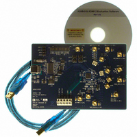
Manufacturer Part Number
AD9912/PCBZ
Description
Eval Board
Manufacturer
Analog Devices Inc
Series
AgileRF™r
Specifications of AD9912/PCBZ
Kit Features
Flexible System Clock I/P Accepts Crystal
Supported Devices
AD9912
Tool / Board Applications
Direct Digital Synthesizer
Development Tool Type
Hardware - Eval/Demo Board
Mcu Supported Families
AD9912
Main Purpose
Timing, Direct Digital Synthesis (DDS)
Embedded
No
Utilized Ic / Part
AD9912
Primary Attributes
14-Bit DAC, 48-Bit Tuning Word Width
Secondary Attributes
1GHz, Graphical User Interface
Lead Free Status / RoHS Status
Lead free / RoHS Compliant
Lead Free Status / RoHS Status
Lead free / RoHS Compliant, Lead free / RoHS Compliant


Because the DAC constitutes a sampled system, its output must
be filtered so that the analog waveform accurately represents the
digital samples supplied to the DAC input. The unfiltered DAC
output contains the (typically) desired baseband signal, which
extends from dc to the Nyquist frequency (f
images of the baseband signal that theoretically extend to infinity.
Notice that the odd images (shown in Figure 42) are mirror
images of the baseband signal. Furthermore, the entire DAC
output spectrum is affected by a sin(x)/x response, which is
caused by the sample-and-hold nature of the DAC output signal.
For applications using the fundamental frequency of the DAC
output, the response of the reconstruction filter should preserve
the baseband signal (Image 0), while completely rejecting all
other images. However, a practical filter implementation
typically exhibits a relatively flat pass band that covers the
desired output frequency plus 20%, rolls off as steeply as
possible, and then maintains significant (though not complete)
rejection of the remaining images. Depending on how close
unwanted spurs are to the desired signal, a third-, fifth-, or
seventh-order elliptic low-pass filter is common.
Some applications operate off an image above the Nyquist
frequency, and those applications use a band-pass filter instead
of a low-pass filter.
The design of the reconstruction filter has a significant impact
on the overall signal performance. Therefore, good filter design
and implementation techniques are important for obtaining the
best possible jitter results.
MAGNITUDE
–100
–20
–40
–60
–80
0
(dB)
BASE BAND
IMAGE 0
SPURS
PRIMARY
SIGNAL
S
Figure 42. DAC Spectrum vs. Reconstruction Filter Response
/2). It also contains
f
s
/2
RESPONSE
FILTER
IMAGE 1
Rev. F | Page 19 of 40
f
s
IMAGE 2
3
f
FDBK_IN INPUTS
The FDBK_IN pins serve as the input to the comparators and
output drivers of the AD9912. Typically, these pins are used to
receive the signal generated by the DDS after it has been band-
limited by the external reconstruction filter.
A diagram of the FDBK_IN input pins is provided in Figure 43,
which includes some of the internal components used to bias
the input circuitry. Note that the FDBK_IN input pins are
internally biased to a dc level of ~1 V. Care should be taken to
ensure that any external connections do not disturb the dc bias
because this may significantly degrade performance.
s
/2
ENVELOPE
SIN(x)/x
IMAGE 3
FDBK_INB
FDBK_IN
2
f
s
Figure 43. Differential FDBK_IN Inputs
AVSS
IMAGE 4
~1pF
~1pF
5
f
s
/2
+
~1V
f
15kΩ
15kΩ
OUTPUT SECTION
~2pF
TO S-DIVIDER
AND CLOCK
AVSS
AD9912
Related parts for AD9912/PCBZ
Image
Part Number
Description
Manufacturer
Datasheet
Request
R


Part Number:
Description:
±1.7g Dual-Axis IMEMS Accelerometer Evaluation Board
Manufacturer:
Analog Devices Inc
Datasheet:

Part Number:
Description:
Inertial Sensor Evaluation System
Manufacturer:
Analog Devices Inc
Datasheet:
Part Number:
Description:
Manufacturer:
Analog Devices Inc
Datasheet:
Part Number:
Description:
Manufacturer:
Analog Devices Inc
Datasheet:
Part Number:
Description:
Manufacturer:
Analog Devices Inc
Datasheet:
Part Number:
Description:
Manufacturer:
Analog Devices Inc
Datasheet:
Part Number:
Description:
Manufacturer:
Analog Devices Inc
Datasheet:
Part Number:
Description:
Manufacturer:
Analog Devices Inc
Datasheet:
Part Number:
Description:
Manufacturer:
Analog Devices Inc
Datasheet:
Part Number:
Description:
Manufacturer:
Analog Devices Inc
Datasheet:
Part Number:
Description:
Manufacturer:
Analog Devices Inc
Datasheet:
Part Number:
Description:
Manufacturer:
Analog Devices Inc
Datasheet: