AD9912/PCBZ Analog Devices Inc, AD9912/PCBZ Datasheet - Page 5
AD9912/PCBZ
Manufacturer Part Number
AD9912/PCBZ
Description
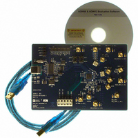
Eval Board
Manufacturer
Analog Devices Inc
Series
AgileRF™r
Specifications of AD9912/PCBZ
Kit Features
Flexible System Clock I/P Accepts Crystal
Supported Devices
AD9912
Tool / Board Applications
Direct Digital Synthesizer
Development Tool Type
Hardware - Eval/Demo Board
Mcu Supported Families
AD9912
Main Purpose
Timing, Direct Digital Synthesis (DDS)
Embedded
No
Utilized Ic / Part
AD9912
Primary Attributes
14-Bit DAC, 48-Bit Tuning Word Width
Secondary Attributes
1GHz, Graphical User Interface
Lead Free Status / RoHS Status
Lead free / RoHS Compliant
Lead Free Status / RoHS Status
Lead free / RoHS Compliant, Lead free / RoHS Compliant


Parameter
SYSTEM CLOCK INPUT
CLOCK OUTPUT DRIVERS
TOTAL POWER DISSIPATION
1
2
Pin 14 is in the AVDD3 group, but it is recommended that Pin 14 be tied to Pin 1.
AVSS = 0 V.
SYSCLK PLL Bypassed
SYSCLK PLL Enabled
Crystal Resonator with SYSCLK PLL Enabled
HSTL Output Driver
CMOS Output Driver
DDS Only
DDS with Spur Reduction On
DDS with HSTL Driver Enabled
DDS with CMOS Driver Enabled
DDS with HSTL and CMOS Drivers Enabled
DDS with SYSCLK PLL Enabled
Power-Down Mode
Input Capacitance
Input Resistance
Internally Generated DC Bias Voltage
Differential Input Voltage Swing
Input Capacitance
Input Resistance
Internally Generated DC Bias Voltage
Differential Input Voltage Swing
Motional Resistance
Differential Output Voltage Swing
Common-Mode Output Voltage
Output Voltage High (V
Output Voltage Low (V
Output Voltage High (V
Output Voltage Low (V
OL
OL
OH
OH
)
)
)
)
2
2
2
Min
2.4
0.93
632
2.4
0.93
632
1080
0.7
2.7
1.4
Typ
1.5
2.6
1.17
3
2.6
1.17
9
1280
0.88
637
686
657
729
747
648
13
Rev. F | Page 5 of 40
0.4
0.4
Max
2.9
1.38
2.9
1.38
100
1480
1.06
765
823
788
875
897
777
16
Unit
pF
kΩ
V
mV p-p
pF
kΩ
V
mV p-p
Ω
mV
V
V
V
V
V
mW
mW
mW
mW
mW
mW
mW
Test Conditions/Comments
System clock inputs should always be ac-
coupled (both single-ended and differential)
Single-ended, each pin
Differential
Equivalent to 316 mV swing on each leg
Single-ended, each pin
Differential
Equivalent to 316 mV swing on each leg
25 MHz, 3.2 mm × 2.5 mm AT cut
Output driver static, see Figure 27 for
output swing vs. frequency
Output driver static, see Figure 28 and
Figure 29 for output swing vs. frequency
I
I
I
I
Power-on default, except SYSCLK PLL by-
passed and CMOS driver off; SYSCLK = 1 GHz;
HSTL driver off; spur reduction off; f
200 MHz
Same as “DDS Only” case, except both spur
reduction channels on
Same as “DDS Only” case, except HSTL driver
enabled
Same as “DDS Only” case, except CMOS
driver and S-divider enabled and at 3.3 V;
CMOS f
Same as “DDS Only” case, except both HSTL
and CMOS drivers enabled; S-divider
enabled and set to 4; CMOS f
Same as “DDS Only” case, except 25 MHz on
SYCLK input and PLL multiplier = 40
Using either the power-down and enable
register or the PWRDOWN pin
OH
OL
OH
OL
= 1 mA, Pin 37 = 3.3 V
= 1 mA, Pin 37 = 1.8 V
= 1 mA, Pin 37 = 3.3 V
= 1 mA, Pin 37 = 1.8 V
OUT
= 50 MHz (S-divider = 4)
OUT
AD9912
= 50 MHz
OUT
=
Related parts for AD9912/PCBZ
Image
Part Number
Description
Manufacturer
Datasheet
Request
R


Part Number:
Description:
±1.7g Dual-Axis IMEMS Accelerometer Evaluation Board
Manufacturer:
Analog Devices Inc
Datasheet:

Part Number:
Description:
Inertial Sensor Evaluation System
Manufacturer:
Analog Devices Inc
Datasheet:
Part Number:
Description:
Manufacturer:
Analog Devices Inc
Datasheet:
Part Number:
Description:
Manufacturer:
Analog Devices Inc
Datasheet:
Part Number:
Description:
Manufacturer:
Analog Devices Inc
Datasheet:
Part Number:
Description:
Manufacturer:
Analog Devices Inc
Datasheet:
Part Number:
Description:
Manufacturer:
Analog Devices Inc
Datasheet:
Part Number:
Description:
Manufacturer:
Analog Devices Inc
Datasheet:
Part Number:
Description:
Manufacturer:
Analog Devices Inc
Datasheet:
Part Number:
Description:
Manufacturer:
Analog Devices Inc
Datasheet:
Part Number:
Description:
Manufacturer:
Analog Devices Inc
Datasheet:
Part Number:
Description:
Manufacturer:
Analog Devices Inc
Datasheet: