AD9912/PCBZ Analog Devices Inc, AD9912/PCBZ Datasheet - Page 2
AD9912/PCBZ
Manufacturer Part Number
AD9912/PCBZ
Description
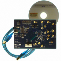
Eval Board
Manufacturer
Analog Devices Inc
Series
AgileRF™r
Specifications of AD9912/PCBZ
Kit Features
Flexible System Clock I/P Accepts Crystal
Supported Devices
AD9912
Tool / Board Applications
Direct Digital Synthesizer
Development Tool Type
Hardware - Eval/Demo Board
Mcu Supported Families
AD9912
Main Purpose
Timing, Direct Digital Synthesis (DDS)
Embedded
No
Utilized Ic / Part
AD9912
Primary Attributes
14-Bit DAC, 48-Bit Tuning Word Width
Secondary Attributes
1GHz, Graphical User Interface
Lead Free Status / RoHS Status
Lead free / RoHS Compliant
Lead Free Status / RoHS Status
Lead free / RoHS Compliant, Lead free / RoHS Compliant


AD9912
TABLE OF CONTENTS
Features .............................................................................................. 1
Applications ....................................................................................... 1
General Description ......................................................................... 1
Basic Block Diagram ........................................................................ 1
Revision History ............................................................................... 3
Specifications ..................................................................................... 4
Absolute Maximum Ratings ............................................................ 8
Pin Configuration and Function Descriptions ............................. 9
Typical Performance Characteristics ........................................... 11
Input/Output Termination Recommendations .......................... 16
Theory of Operation ...................................................................... 17
Thermal Performance .................................................................... 24
Power-Up ......................................................................................... 25
DC Specifications ......................................................................... 4
AC Specifications .......................................................................... 6
Thermal Resistance ...................................................................... 8
ESD Caution .................................................................................. 8
Overview ...................................................................................... 17
Direct Digital Synthesizer (DDS) ............................................. 17
Digital-to-Analog (DAC) Output ............................................ 18
Reconstruction Filter ................................................................. 18
FDBK_IN Inputs ........................................................................ 19
SYSCLK Inputs ........................................................................... 20
Output Clock Drivers and 2× Frequency Multiplier ............. 22
Harmonic Spur Reduction ........................................................ 22
Power-On Reset .......................................................................... 25
Rev. F | Page 2 of 40
Power Supply Partitioning ............................................................. 26
Serial Control Port ......................................................................... 27
I/O Register Map ............................................................................ 31
I/O Register Descriptions .............................................................. 33
Outline Dimensions ....................................................................... 39
Default Output Frequency on Power-Up ................................ 25
3.3 V Supplies .............................................................................. 26
1.8 V Supplies .............................................................................. 26
Serial Control Port Pin Descriptions ....................................... 27
Operation of Serial Control Port .............................................. 27
The Instruction Word (16 Bits) ................................................ 28
MSB/LSB First Transfers ........................................................... 28
Serial Port Configuration (Register 0x0000 to
Register 0x0005) ......................................................................... 33
Power-Down and Reset (Register 0x0010 to
Register 0x0013) ......................................................................... 33
System Clock (Register 0x0020 to Register 0x0022) ............. 34
CMOS Output Divider (S-Divider) (Register 0x0100 to
Register 0x0106) ......................................................................... 35
Frequency Tuning Word (Register 0x01A0 to
Register 0x01AD) ....................................................................... 35
Doubler and Output Drivers (Register 0x0200 to
Register 0x0201) ......................................................................... 37
Calibration (User-Accessible Trim) (Register 0x0400 to
Register 0x0410) ......................................................................... 37
Harmonic Spur Reduction (Register 0x0500 to
Register 0x0509) ......................................................................... 37
Ordering Guide .......................................................................... 39
Related parts for AD9912/PCBZ
Image
Part Number
Description
Manufacturer
Datasheet
Request
R


Part Number:
Description:
±1.7g Dual-Axis IMEMS Accelerometer Evaluation Board
Manufacturer:
Analog Devices Inc
Datasheet:

Part Number:
Description:
Inertial Sensor Evaluation System
Manufacturer:
Analog Devices Inc
Datasheet:
Part Number:
Description:
Manufacturer:
Analog Devices Inc
Datasheet:
Part Number:
Description:
Manufacturer:
Analog Devices Inc
Datasheet:
Part Number:
Description:
Manufacturer:
Analog Devices Inc
Datasheet:
Part Number:
Description:
Manufacturer:
Analog Devices Inc
Datasheet:
Part Number:
Description:
Manufacturer:
Analog Devices Inc
Datasheet:
Part Number:
Description:
Manufacturer:
Analog Devices Inc
Datasheet:
Part Number:
Description:
Manufacturer:
Analog Devices Inc
Datasheet:
Part Number:
Description:
Manufacturer:
Analog Devices Inc
Datasheet:
Part Number:
Description:
Manufacturer:
Analog Devices Inc
Datasheet:
Part Number:
Description:
Manufacturer:
Analog Devices Inc
Datasheet: