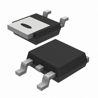
BUK9240-100A,118 NXP Semiconductors, BUK9240-100A,118 Datasheet - Page 5

BUK9240-100A,118
Manufacturer Part Number
BUK9240-100A,118
Description
MOSFET N-CH 100V 33A DPAK
Manufacturer
NXP Semiconductors
Series
TrenchMOS™r
Specifications of BUK9240-100A,118
Package / Case
DPak, TO-252 (2 leads+tab), SC-63
Fet Type
MOSFET N-Channel, Metal Oxide
Fet Feature
Logic Level Gate
Rds On (max) @ Id, Vgs
38.6 mOhm @ 25A, 10V
Drain To Source Voltage (vdss)
100V
Current - Continuous Drain (id) @ 25° C
33A
Vgs(th) (max) @ Id
2V @ 1mA
Input Capacitance (ciss) @ Vds
3072pF @ 25V
Power - Max
114W
Mounting Type
Surface Mount
Minimum Operating Temperature
- 55 C
Configuration
Single
Transistor Polarity
N-Channel
Resistance Drain-source Rds (on)
0.0386 Ohm @ 10 V
Drain-source Breakdown Voltage
100 V
Gate-source Breakdown Voltage
+/- 10 V
Continuous Drain Current
33 A
Power Dissipation
114000 mW
Maximum Operating Temperature
+ 175 C
Mounting Style
SMD/SMT
Lead Free Status / RoHS Status
Lead free / RoHS Compliant
Gate Charge (qg) @ Vgs
-
Lead Free Status / Rohs Status
Lead free / RoHS Compliant
Other names
934056252118
BUK9240-100A /T3
BUK9240-100A /T3
BUK9240-100A /T3
BUK9240-100A /T3
8. Characteristics
Table 5:
T
Philips Semiconductors
9397 750 07573
Product specification
Symbol
Static characteristics
V
V
I
I
R
Dynamic characteristics
C
C
C
t
t
t
t
L
L
DSS
GSS
d(on)
r
d(off
f
j
d
s
(BR)DSS
GS(th)
DSon
iss
oss
rss
= 25 C unless otherwise specified
)
Characteristics
Parameter
drain-source breakdown
voltage
gate-source threshold voltage I
drain-source leakage current
gate-source leakage current
drain-source on-state
resistance
input capacitance
output capacitance
reverse transfer capacitance
turn-on delay time
rise time
turn-off delay time
fall time
internal drain inductance
internal source inductance
Conditions
I
Figure 9
V
V
V
Figure 7
V
T
V
T
V
f = 1 MHz;
V
V
measured from drain lead
from package to centre of
die
measured from source lead
from package to source
bond pad
D
D
GS
j
GS
j
DS
GS
GS
GS
DD
GS
T
T
T
T
T
T
T
T
T
= 0.25 mA; V
= 1 mA; V
= 25 C
=25 C
j
j
j
j
j
j
j
j
j
= 100 V; V
= 25 C
= 55 C
= 25 C
= 175 C
= 55 C
= 25 C
= 175 C
= 10 V; V
= 5 V; I
= 25 C
= 175 C
= 4.5 V; I
= 10 V; I
= 0 V; V
= 30 V; R
= 5 V; R
Rev. 01 — 03 October 2000
and
Figure 12
D
DS
DS
G
D
8
= 25 A;
D
L
=25 A;
= 10
GS
DS
= V
= 25 A;
GS
= 25 V;
= 1.2 ;
= 0 V
= 0 V
= 0 V
GS
;
Min
100
89
1
0.5
BUK9240-100A
TrenchMOS™ logic level FET
Typ
1.5
0.05
2
34
33
2304
222
151
20
135
125
90
2.5
7.5
© Philips Electronics N.V. 2000. All rights reserved.
Max
2
2.3
10
500
100
40
100
44.6
38.6
3072
266.4
207
Unit
V
V
V
V
V
nA
m
m
m
m
pF
pF
pF
ns
ns
ns
ns
nH
nH
5 of 13
A
A


