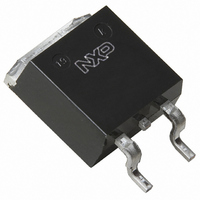
BUK9610-55A,118 NXP Semiconductors, BUK9610-55A,118 Datasheet

BUK9610-55A,118
Specifications of BUK9610-55A,118
BUK9610-55A /T3
BUK9610-55A /T3
Related parts for BUK9610-55A,118
BUK9610-55A,118 Summary of contents
Page 1
... BUK9610-55A N-channel TrenchMOS logic level FET Rev. 02 — 16 February 2011 1. Product profile 1.1 General description Logic level N-channel enhancement mode Field-Effect Transistor (FET plastic package using TrenchMOS technology. This product has been designed and qualified to the appropriate AEC standard for use in automotive critical applications. ...
Page 2
... see Figure 13 Simplified outline SOT404 (D2PAK) Description plastic single-ended surface-mounted package (D2PAK); 3 leads (one lead cropped) All information provided in this document is subject to legal disclaimers. Rev. 02 — 16 February 2011 BUK9610-55A N-channel TrenchMOS logic level FET Min ≤ sup = °C; j Graphic symbol G mbb076 ...
Page 3
... sup °C; unclamped GS j(init) 03nf89 120 P der (%) 150 175 200 T (°C) mb Fig 2. All information provided in this document is subject to legal disclaimers. Rev. 02 — 16 February 2011 BUK9610-55A N-channel TrenchMOS logic level FET Min - - -15 [1] Figure 1; - [2] - [1] Figure 1 - ≤ 10 µ -55 -55 [ ° Ω; ...
Page 4
... DSon δ Conditions see Figure 4 mounted on printed-circuit board; minimum footprint −5 −4 − All information provided in this document is subject to legal disclaimers. Rev. 02 — 16 February 2011 BUK9610-55A N-channel TrenchMOS logic level FET 03nf86 = 10 μ 100 μ 100 (V) DS Min Typ - - - 50 03nf87 t p δ = ...
Page 5
... °C j from upper edge of drain mounting base to centre of die °C j from source lead to source bond pad °C j All information provided in this document is subject to legal disclaimers. Rev. 02 — 16 February 2011 BUK9610-55A N-channel TrenchMOS logic level FET Min Typ Max 1 ...
Page 6
... ° 03nd75 2 (V) DS Fig 6. 03aa36 max (V) GS Fig 8. All information provided in this document is subject to legal disclaimers. Rev. 02 — 16 February 2011 BUK9610-55A N-channel TrenchMOS logic level FET Min - = DSon (mΩ Drain-source on-state resistance as a function of gate-source voltage; typical values ( Forward transconductance as a function of drain current ...
Page 7
... Fig 10. Gate-source threshold voltage as a function of 03nd76 3 150 200 250 I (A) D Fig 12. Normalized drain-source on-state resistance All information provided in this document is subject to legal disclaimers. Rev. 02 — 16 February 2011 BUK9610-55A N-channel TrenchMOS logic level FET 2.5 V GS(th) (V) 2 max 1.5 typ min 1 0.5 0 ...
Page 8
... Fig 14. Input, output and reverse transfer capacitances 100 175 ° 0.5 1.0 All information provided in this document is subject to legal disclaimers. Rev. 02 — 16 February 2011 BUK9610-55A N-channel TrenchMOS logic level FET C iss C oss C rss 0 −2 − function of drain-source voltage; typical values 03nd70 = 25 ° ...
Page 9
... REFERENCES JEDEC JEITA All information provided in this document is subject to legal disclaimers. Rev. 02 — 16 February 2011 BUK9610-55A N-channel TrenchMOS logic level FET mounting base 2.60 2.20 EUROPEAN ISSUE DATE PROJECTION 05-02-11 06-03-16 © ...
Page 10
... The format of this data sheet has been redesigned to comply with the new identity guidelines of NXP Semiconductors. • Legal texts have been adapted to the new company name where appropriate. • Type number BUK9610-55A separated from data sheet BUK9510_9610_55A v.1. BUK9510_9610_55A v.1 20010820 BUK9610-55A Product data sheet Data sheet status ...
Page 11
... In case an individual All information provided in this document is subject to legal disclaimers. Rev. 02 — 16 February 2011 BUK9610-55A N-channel TrenchMOS logic level FET © NXP B.V. 2011. All rights reserved ...
Page 12
... TrenchMOS, TriMedia and UCODE — are trademarks of NXP B.V. HD Radio and HD Radio logo — are trademarks of iBiquity Digital Corporation. http://www.nxp.com salesaddresses@nxp.com All information provided in this document is subject to legal disclaimers. Rev. 02 — 16 February 2011 BUK9610-55A N-channel TrenchMOS logic level FET Trademarks © NXP B.V. 2011. All rights reserved ...
Page 13
... Please be aware that important notices concerning this document and the product(s) described herein, have been included in section ‘Legal information’. © NXP B.V. 2011. For more information, please visit: http://www.nxp.com For sales office addresses, please send an email to: salesaddresses@nxp.com All rights reserved. Date of release: 16 February 2011 Document identifier: BUK9610-55A ...


