IRF3808SPBF International Rectifier, IRF3808SPBF Datasheet
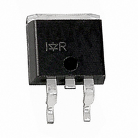
MOSFET N-CH 75V 106A D2PAK

IRF3808SPBF

Manufacturer Part Number
IRF3808SPBF
Description
MOSFET N-CH 75V 106A D2PAK
Manufacturer
International Rectifier
Series
HEXFET®r
Datasheets

Specifications of IRF3808SPBF

Fet Type
MOSFET N-Channel, Metal Oxide
Fet Feature
Standard
Rds On (max) @ Id, Vgs
7 mOhm @ 82A, 10V
Drain To Source Voltage (vdss)
75V
Current - Continuous Drain (id) @ 25° C
106A
Vgs(th) (max) @ Id
4V @ 250µA
Gate Charge (qg) @ Vgs
220nC @ 10V
Input Capacitance (ciss) @ Vds
5310pF @ 25V
Power - Max
200W
Mounting Type
Surface Mount
Package / Case
D²Pak, TO-263 (2 leads + tab)
Current, Drain
106 A
Gate Charge, Total
150 nC
Package Type
D2Pak
Polarization
N-Channel
Power Dissipation
200 W
Resistance, Drain To Source On
5.9 Milliohms
Temperature, Operating, Maximum
+175 °C
Temperature, Operating, Minimum
-55 °C
Time, Turn-off Delay
68 ns
Time, Turn-on Delay
16 ns
Transconductance, Forward
100 S
Voltage, Breakdown, Drain To Source
75 V
Voltage, Forward, Diode
1.3 V
Voltage, Gate To Source
±20 V
Lead Free Status / RoHS Status
Lead free / RoHS Compliant
Other names
*IRF3808SPBF
Benefits
Absolute Maximum Ratings
Thermal Resistance
HEXFET(R) is a registered trademark of International Rectifier.
Typical Applications
This Advanced Planar Stripe HEXFET ® Power MOSFET utilizes
the latest processing techniques to achieve extremely low on-
resistance per silicon area. Additional features of this HEXFET
power MOSFET are a 175°C junction operating temperature, low
R JC, fast switching speed and improved repetitive avalanche
rating. This combination makes the design an extremely efficient
and reliable choice for use in a wide variety of applications.
Description
www.irf.com
I
I
I
P
V
E
I
E
dv/dt
T
T
R
R
D
D
DM
AR
J
STG
D
GS
AS
AR
@ T
@ T
JC
JA
@T
Industrial Motor Drive
Advanced Process Technology
Ultra Low On-Resistance
Dynamic dv/dt Rating
175°C Operating Temperature
Fast Switching
Repetitive Avalanche Allowed up to Tjmax
Lead-Free
C
C
C
= 25°C
= 100°C
= 25°C
Continuous Drain Current, V
Pulsed Drain Current 
Power Dissipation
Linear Derating Factor
Gate-to-Source Voltage
Single Pulse Avalanche Energy‚
Avalanche Current
Repetitive Avalanche Energy‡
Peak Diode Recovery dv/dt ƒ
Operating Junction and
Storage Temperature Range
Soldering Temperature, for 10 seconds
Junction-to-Case
Junction-to-Ambient
Parameter
Parameter
(PCB Mounted, Steady State)**
GS
GS
@ 10V
@ 10V
G
See Fig.12a, 12b, 15, 16
Typ.
300 (1.6mm from case )
–––
–––
IRF3808SPbF
IRF3808LPbF
HEXFET
-55 to + 175
IRF3808SPbF
D
S
Max.
106†
75†
550
200
± 20
430
1.3
5.5
82
D
2
Pak
®
R
Power MOSFET
DS(on)
Max.
I
V
0.75
D
40
DSS
= 106A†
IRF3808LPbF
PD - 95467A
= 0.007
= 75V
TO-262
Units
Units
W/°C
°C/W
V/ns
mJ
mJ
°C
W
A
V
A
1

Related parts for IRF3808SPBF

IRF3808SPBF Summary of contents

Page 1

... Typ. ––– ––– (PCB Mounted, Steady State)** PD - 95467A ® HEXFET Power MOSFET 75V DSS R = 0.007 DS(on 106A† Pak TO-262 IRF3808SPbF IRF3808LPbF Max. Units 106† 75† A 550 200 W 1.3 W/°C ± 430 5.5 V/ns - 175 °C Max ...

Page 2

IRF3808S/LPbF Electrical Characteristics @ T Parameter V Drain-to-Source Breakdown Voltage (BR)DSS Breakdown Voltage Temp. Coefficient (BR)DSS J R Static Drain-to-Source On-Resistance DS(on) V Gate Threshold Voltage GS(th) g Forward Transconductance fs I Drain-to-Source Leakage Current DSS Gate-to-Source ...

Page 3

VGS TOP 15V 10V 8.0V 7.0V 6.0V 5.5V 5.0V BOTTOM 4.5V 100 4.5V 10 20µs PULSE WIDTH 0 Drain-to-Source Voltage (V) DS Fig 1. Typical Output Characteristics 1000.00 100. ...

Page 4

IRF3808S/LPbF 100000 0V, C iss = rss = oss = 10000 Coss 1000 Crss 100 ...

Page 5

LIMITED BY PACKAGE 100 100 125 T , Case Temperature C Fig 9. Maximum Drain Current Vs. Case Temperature 0.50 0.20 0.1 0.10 0.05 0.02 SINGLE PULSE 0.01 ...

Page 6

IRF3808S/LPbF D.U 20V 0. Fig 12a. Unclamped Inductive Test Circuit V (BR)DSS Fig 12b. Unclamped Inductive Waveforms Charge Fig ...

Page 7

Duty Cycle = Single Pulse 100 0.01 0.05 10 0.10 1 0.1 1.0E-07 1.0E-06 Fig 15. Typical Avalanche Current Vs.Pulsewidth 500 TOP Single Pulse BOTTOM 10% Duty Cycle 140A 400 300 200 100 0 25 ...

Page 8

IRF3808S/LPbF D.U.T + ‚ -  Driver Gate Drive P.W. D.U.T. I Reverse Recovery Current D.U.T. V Re-Applied Voltage Inductor Curent 8 + ƒ Period D = Waveform SD Body Diode Forward Current di/dt Waveform DS Diode Recovery ...

Page 9

T HIS IS AN IRF530S WITH LOT CODE 8024 ASSEMBLED ON WW 02, 2000 IN THE ASS EMBLY LINE "L" OR Notes: 1. For an Automotive Qualified version of this part please see http://www.irf.com/product-info/auto/ 2. For the most ...

Page 10

IRF3808S/LPbF TO-262 Package Outline Dimensions are shown in millimeters (inches) TO-262 Part Marking Information EXAMPLE: THIS IS AN IRL3103L LOT CODE 1789 ASS EMBLED ON WW 19, 1997 ASSEMBLY LINE "C" Note: "P" in assembly line position ...

Page 11

TRR FEED DIRECTION 1.85 (.073) 1.65 (.065) TRL 10.90 (.429) 10.70 (.421) FEED DIRECTION 13.50 (.532) 12.80 (.504) 330.00 (14.173) MAX. NOTES : 1. COMFORMS TO EIA-418. 2. CONTROLLING DIMENSION: MILLIMETER. 3. DIMENSION MEASURED @ HUB. 4. INCLUDES FLANGE ...

Related keywords