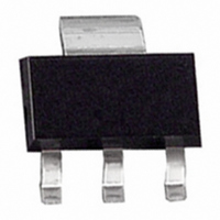
BSP315P-E6327 Infineon Technologies, BSP315P-E6327 Datasheet - Page 2

BSP315P-E6327
Manufacturer Part Number
BSP315P-E6327
Description
MOSFET P-CH 60V 1.17A SOT-223
Manufacturer
Infineon Technologies
Series
SIPMOS®r
Datasheet
1.BSP315P_L6327.pdf
(9 pages)
Specifications of BSP315P-E6327
Fet Type
MOSFET P-Channel, Metal Oxide
Fet Feature
Logic Level Gate
Rds On (max) @ Id, Vgs
800 mOhm @ 1.17A, 10V
Drain To Source Voltage (vdss)
60V
Current - Continuous Drain (id) @ 25° C
1.17A
Vgs(th) (max) @ Id
2V @ 160µA
Gate Charge (qg) @ Vgs
7.8nC @ 10V
Input Capacitance (ciss) @ Vds
160pF @ 25V
Power - Max
1.8W
Mounting Type
Surface Mount
Package / Case
SOT-223 (3 leads + Tab), SC-73, TO-261
Lead Free Status / RoHS Status
Contains lead / RoHS non-compliant
Other names
BSP315P
BSP315PINTR
BSP315PINTR
Electrical Characteristics, at T
Parameter
Static Characteristics
Drain- source breakdown voltage
V
Gate threshold voltage, V
I
Zero gate voltage drain current
V
V
Gate-source leakage current
V
Drain-Source on-state resistance
V
Drain-Source on-state resistance
V
1 Device on 40mm*40mm*1.5mm epoxy PCB FR4 with 6cm 2 (one layer, 70 µm thick) copper area for drain
connection. PCB is vertical without blown air.
Thermal Characteristics
Parameter
Characteristics
Thermal resistance, junction - soldering point
(Pin 4)
SMD version, device on PCB:
@ min. footprint
@ 6 cm
D
Rev.1.4
GS
DS
DS
GS
GS
GS
= -160 µA
= -60 V, V
= -60 V, V
= 0 V, I
= -20 V, V
= -4.5 V, I
= -10 V, I
2
cooling area
D
= -250 µA
D
D
GS
GS
DS
= -1.17 A
= -0.89 A
= 0 V, T
= 0 V, T
= 0 V
1)
GS
j
j
= 25 °C
= 125 °C
= V
j
DS
= 25 °C, unless otherwise specified
Page 2
Symbol
V
V
I
I
R
R
Symbol
R
R
DSS
GSS
(BR)DSS
GS(th)
DS(on)
DS(on)
thJS
thJA
min.
min.
-60
-1
-
-
-
-
-
-
-
-
Values
Values
typ.
-1.5
-0.1
typ.
-10
-10
0.8
0.5
-
-
-
-
max.
max.
-100
-100
115
BSP 315 P
1.4
0.8
25
70
-2
-1
2007-02-08
-
Unit
V
µA
nA
Unit
K/W
K/W


