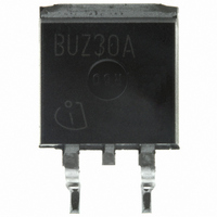
BUZ30A H3045A Infineon Technologies, BUZ30A H3045A Datasheet

BUZ30A H3045A
Specifications of BUZ30A H3045A
BUZ30A L3045A
BUZ30AH3045AINTR
BUZ30AL3045AINTR
BUZ30AL3045AINTR
BUZ30AL3045AXT
SP000102176
SP000736082
Related parts for BUZ30A H3045A
BUZ30A H3045A Summary of contents
Page 1
SIPMOS Power Transistor • N channel • Enhancement mode • Avalanche-rated . Halogen-free according to IEC61249-2--21 Type V DS BUZ 30A H 200 V Maximum Ratings Parameter Continuous drain current ˚C C Pulsed drain current T ...
Page 2
Electrical Characteristics Parameter Static Characteristics Drain- source breakdown voltage 0.25 mA ˚ Gate threshold voltage DS, D Zero ...
Page 3
Electrical Characteristics Parameter Dynamic Characteristics Transconductance ≥ 13 DS(on)max, D Input capacitance MHz GS DS Output ...
Page 4
Electrical Characteristics Parameter Reverse Diode Inverse diode continuous forward current ˚C C Inverse diode direct current,pulsed ˚C C Inverse diode forward voltage ...
Page 5
Power dissipation = ƒ tot C 130 W 110 P tot 100 Safe operating area = ƒ ...
Page 6
Typ. output characteristics = ƒ parameter µ 125W tot ...
Page 7
Drain-source on-resistance = ƒ (on) j parameter 13 0.50 Ω 0. (on) 0.35 0.30 0.25 0.20 98% typ 0.15 0.10 0.05 0.00 -60 -20 ...
Page 8
T Avalanche energy E AS parameter Ω 1. 500 mJ 400 E AS 350 300 250 200 150 100 ...
Page 9
Package Drawing: TO220-3 Rev. 2.5 Page 9 BUZ 30A H 2010-07-02 ...
Page 10
... Infineon Technologies Office. Infineon Technologies components may be used in life-support devices or systems only with the express written approval of Infineon Technologies failure of such components can reasonably be expected to cause the failure of that life-support device or system or to affect the safety or effectiveness of that device or system ...


