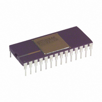
AD676BD Analog Devices Inc, AD676BD Datasheet - Page 2

AD676BD
Manufacturer Part Number
AD676BD
Description
ADC Single SAR 100KSPS 16-Bit Parallel 28-Pin SBCDIP
Manufacturer
Analog Devices Inc
Datasheet
1.AD676JNZ.pdf
(16 pages)
Specifications of AD676BD
Package
28SBCDIP
Resolution
16 Bit
Sampling Rate
100 KSPS
Architecture
SAR
Number Of Analog Inputs
1
Digital Interface Type
Parallel
Input Type
Voltage
Polarity Of Input Voltage
Bipolar
Rohs Status
RoHS non-compliant
Number Of Bits
16
Sampling Rate (per Second)
100k
Data Interface
Parallel
Number Of Converters
2
Power Dissipation (max)
480mW
Voltage Supply Source
Analog and Digital, Dual ±
Operating Temperature
-40°C ~ 85°C
Mounting Type
Through Hole
Package / Case
28-CDIP (0.600", 15.24mm)
For Use With
AD676-EB - BOARD EVAL SAMPLING ADC AD676
Lead Free Status / RoHS Status
Available stocks
Company
Part Number
Manufacturer
Quantity
Price
Part Number:
AD676BD
Manufacturer:
ADI/亚德诺
Quantity:
20 000
AD676–SPECIFICATIONS
AC SPECIFICATIONS
Parameter
Total Harmonic Distortion (THD)
Signal-to-Noise and Distortion Ratio (S/(N+D))
Peak Spurious or Peak Harmonic Component
Intermodulation Distortion (IMD)
Full Power Bandwidth
Noise
DIGITAL SPECIFICATIONS
Parameter
LOGIC INPUTS
V
V
I
I
C
LOGIC OUTPUTS
V
V
NOTES
1
2
3
4
Specifications subject to change without notice.
V
For other input amplitudes, refer to Figure 13.
For other input ranges/voltages reference values see Figure 12.
fa = 1008 Hz. fb = 1055 Hz. See Definition of Specifications section and Figure 15.
IH
IL
(20 V p-p) input signal. Values are post-calibration.
IH
IL
OH
OL
IN
REF
@ 83 kSPS, T
@ 100 kSPS, +25 C
@ 100 kSPS, T
@ 83 kSPS, T
@ 100 kSPS, +25 C
@ 100 kSPS, T
2nd Order Products
3rd Order Products
= 10.0 V, (Conversion Rate (fs) = 83 kSPS, f
High Level Input Voltage
Low Level Input Voltage
High Level Input Current
Low Level Input Current
Input Capacitance
High Level Output Voltage
Low Level Output Voltage
MIN
MIN
MIN
MIN
to T
to T
to T
to T
MAX
MAX
MAX
MAX
(T
MIN
4
2
to T
(for all grades T
MAX,
IN
V
= 1.0 kHz, V
CC
= +12 V
2, 3
Test Conditions
V
V
I
I
I
IN
OH
OH
OL
MIN
IH
IL
= –0.05 dB, Bandwidth = fs/2 unless otherwise indicated. All measurements referred to a 0 dB
= 1.6 mA
= 0 V
= 0.5 mA
5%, V
= 0.1 mA
= V
to T
Min
85
MAX
DD
EE
, V
= –12 V
–2–
CC
AD676J/A
= +12 V
Typ
–96
0.0016
–96
0.0016
–92
0.0025
89
89
86
–98
–102
–98
1
160
5%, V
5%, V
Max
–88
0.004
Min
2.4
–0.3
–10
–10
V
2.4
DD
DD
= +5 V
EE
–1 V
= –12 V
Min
87
10%)
Typ
10
1
AD676K/B
5%, V
Typ
–97
0.0014
–97
0.0014
–92
0.0025
90
90
86
–98
–102
–98
1
160
DD
Max
V
0.8
+10
+10
0.4
= +5 V
DD
+ 0.3
Max
–90
0.003
10%)
V
Units
V
pF
V
V
V
A
A
dB
MHz
Units
dB
%
dB
%
dB
%
dB
dB
dB
dB
dB
REV. A
V rms


