AD676BD Analog Devices Inc, AD676BD Datasheet - Page 6
AD676BD
Manufacturer Part Number
AD676BD
Description
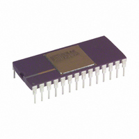
ADC Single SAR 100KSPS 16-Bit Parallel 28-Pin SBCDIP
Manufacturer
Analog Devices Inc
Datasheet
1.AD676JNZ.pdf
(16 pages)
Specifications of AD676BD
Package
28SBCDIP
Resolution
16 Bit
Sampling Rate
100 KSPS
Architecture
SAR
Number Of Analog Inputs
1
Digital Interface Type
Parallel
Input Type
Voltage
Polarity Of Input Voltage
Bipolar
Rohs Status
RoHS non-compliant
Number Of Bits
16
Sampling Rate (per Second)
100k
Data Interface
Parallel
Number Of Converters
2
Power Dissipation (max)
480mW
Voltage Supply Source
Analog and Digital, Dual ±
Operating Temperature
-40°C ~ 85°C
Mounting Type
Through Hole
Package / Case
28-CDIP (0.600", 15.24mm)
For Use With
AD676-EB - BOARD EVAL SAMPLING ADC AD676
Lead Free Status / RoHS Status
Available stocks
Company
Part Number
Manufacturer
Quantity
Price

Part Number:
AD676BD
Manufacturer:
ADI/亚德诺
Quantity:
20 000


AD676
Pin
1–6
7
8
9
10
11
12
13
14
15
16
17
18
19–28
Type: AI = Analog Input
DI = Digital Input
DO = Digital Output
P = Power
Name
BIT 11-BIT 16
BUSY
CAL
SAMPLE
CLK
DGND
V
AGND
AGND SENSE
V
V
V
V
BIT 1–BIT 10
AGND SENSE
CC
IN
REF
EE
DD
BIT 16 (LSB)
SAMPLE
BIT 14
BIT 15
BIT 12
BIT 13
BIT 11
DGND
AGND
BUSY
CAL
CLK
V
CC
12
13
10
11
14
1
2
4
5
7
8
3
6
9
Package Pinout
(Not to Scale)
TOP VIEW
Type
DO
DO
DI
DI
DI
P
P
P/AI
AI
AI
AI
P
P
DO
AD676
Description
BIT 11–BIT 16 represent the six LSBs of data.
Status Line for Converter. Active HIGH, indicating a conversion or calibration in progress.
BUSY should be buffered when capacitively loaded.
Calibration Control Pin (Asynchronous).
V
of the internal sample-hold amplifier and the falling edge initiates conversion (see “Conver-
sion Control” paragraph). During calibration, SAMPLE should be held LOW. If HIGH dur-
ing calibration, diagnostic information will appear on the two LSBs (Pins 5 and 6).
Master Clock Input. The AD676 requires 17 clock cycles to execute a conversion.
Digital Ground.
+12 V Analog Supply Voltage.
Analog Ground.
Analog Ground Sense.
Analog Input Voltage.
External Voltage Reference Input.
–12 V Analog Supply Voltage. Note: the lid of the ceramic package is internally connected to
V
+5 V Logic Supply Voltage.
BIT 1–BIT 10 represent the ten MSB of data.
IN
EE
19
28
27
26
25
24
23
22
20
18
17
16
15
21
.
Acquisition Control Pin. Active HIGH. During conversion, SAMPLE controls the state
BIT 10
BIT 9
BIT 8
BIT 6
BIT 5
BIT 4
BIT 3
BIT 2
BIT 1 (MSB)
V
V
V
BIT 7
V
DD
EE
REF
IN
PIN DESCRIPTION
–6–
AGND SENSE
SAMPLE
AGND
V
CAL
CLK 10
REF
V
IN
15
14
16
16
13
8
9
DIGITAL
CHIP
Functional Block Diagram
BUFFERS
MICRO-CODED
CONTROLLER
INPUT
LEVEL TRANSLATORS
LOGIC & TIMING
CAL
DAC
16-BIT
DAC
RAM
GEN
SAR
PAT
ALU
COMP
ANALOG
AD676
CHIP
A
C
H
L
T
19
28
1
6
7
BUSY
BIT 1 – BIT 16
REV. A
Related parts for AD676BD
Image
Part Number
Description
Manufacturer
Datasheet
Request
R

Part Number:
Description:
BOARD EVAL SAMPLING ADC AD676
Manufacturer:
Analog Devices Inc
Datasheet:

Part Number:
Description:
±1.7g Dual-Axis IMEMS Accelerometer Evaluation Board
Manufacturer:
Analog Devices Inc
Datasheet:
Part Number:
Description:
Inertial Sensor Evaluation System
Manufacturer:
Analog Devices Inc
Datasheet:
Part Number:
Description:
Manufacturer:
Analog Devices Inc
Datasheet:
Part Number:
Description:
Manufacturer:
Analog Devices Inc
Datasheet:
Part Number:
Description:
Manufacturer:
Analog Devices Inc
Datasheet:
Part Number:
Description:
Manufacturer:
Analog Devices Inc
Datasheet:
Part Number:
Description:
Manufacturer:
Analog Devices Inc
Datasheet:
Part Number:
Description:
Manufacturer:
Analog Devices Inc
Datasheet:
Part Number:
Description:
Manufacturer:
Analog Devices Inc
Datasheet:
Part Number:
Description:
Manufacturer:
Analog Devices Inc
Datasheet:
Part Number:
Description:
Manufacturer:
Analog Devices Inc
Datasheet:
Part Number:
Description:
Manufacturer:
Analog Devices Inc
Datasheet: