BLF147,112 NXP Semiconductors, BLF147,112 Datasheet - Page 4
BLF147,112
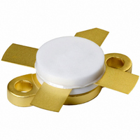
Manufacturer Part Number
BLF147,112
Description
TRANSISTOR RF DMOS SOT121B
Manufacturer
NXP Semiconductors
Datasheet
1.BLF147112.pdf
(15 pages)
Specifications of BLF147,112
Package / Case
SOT-121B
Transistor Type
N-Channel
Frequency
108MHz
Gain
14dB
Voltage - Rated
65V
Current Rating
25A
Voltage - Test
28V
Power - Output
150W
Minimum Operating Temperature
- 65 C
Mounting Style
SMD/SMT
Resistance Drain-source Rds (on)
0.15 Ohm @ 10 V
Transistor Polarity
N-Channel
Configuration
Single Dual Source
Drain-source Breakdown Voltage
65 V
Gate-source Breakdown Voltage
+/- 20 V
Continuous Drain Current
25 A
Power Dissipation
220000 mW
Maximum Operating Temperature
+ 200 C
Application
HF/VHF
Channel Type
N
Channel Mode
Enhancement
Drain Source Voltage (max)
65V
Output Power (max)
150W
Power Gain (typ)@vds
19@28VdB
Frequency (max)
108MHz
Package Type
CRFM
Pin Count
4
Forward Transconductance (typ)
7.5S
Drain Source Resistance (max)
150@10Vmohm
Input Capacitance (typ)@vds
450@28VpF
Output Capacitance (typ)@vds
360@28VpF
Reverse Capacitance (typ)
55@28VpF
Operating Temp Range
-65C to 200C
Drain Efficiency (typ)
40%
Mounting
Screw
Mode Of Operation
SSB Class-AB
Number Of Elements
1
Power Dissipation (max)
220000mW
Vswr (max)
50
Screening Level
Military
Lead Free Status / RoHS Status
Lead free / RoHS Compliant
Noise Figure
-
Current - Test
-
Lead Free Status / Rohs Status
Lead free / RoHS Compliant
Other names
568-2385
933930000112
BLF147
BLF147
933930000112
BLF147
BLF147


NXP Semiconductors
CHARACTERISTICS
T
V
V
I
I
V
g
R
I
C
C
C
j
DSS
GSS
DSX
GS
fs
V
(BR)DSS
GSth
= 25 C unless otherwise specified.
DSon
is
os
rs
VHF power MOS transistor
GS
SYMBOL
group indicator
GROUP
M
C
D
G
H
N
A
B
E
F
K
J
L
drain-source breakdown voltage
drain-source leakage current
gate-source leakage current
gate-source threshold voltage
gate-source voltage difference of
matched pairs
forward transconductance
drain-source on-state resistance
on-state drain current
input capacitance
output capacitance
feedback capacitance
MIN.
2.0
2.1
2.2
2.3
2.4
2.5
2.6
2.7
2.8
2.9
3.0
3.1
3.2
PARAMETER
LIMITS
(V)
MAX.
Rev. 06 - 5 December 2006
2.1
2.2
2.3
2.4
2.5
2.6
2.7
2.8
2.9
3.0
3.1
3.2
3.3
I
V
V
I
I
I
I
V
V
V
V
D
D
D
D
D
GS
GS
GS
GS
GS
GS
= 100 mA; V
= 200 mA; V
= 100 mA; V
= 8 A; V
= 8 A; V
= 0; V
= 20 V; V
= 10 V; V
= 0; V
= 0; V
= 0; V
CONDITIONS
GROUP
DS
DS
GS
DS
DS
DS
W
= 28 V
= 10 V
= 28 V; f = 1 MHz
= 28 V; f = 1 MHz
= 28 V; f = 1 MHz
O
Q
R
U
= 10 V
P
S
T
V
X
Y
Z
DS
GS
DS
DS
DS
= 10 V
= 10 V
= 10 V
= 0
= 0
MIN.
3.3
3.4
3.5
3.6
3.7
3.8
3.9
4.0
4.1
4.2
4.3
4.4
65
2
5
MIN.
LIMITS
7.5
0.1
37
450
360
55
TYP. MAX.
(V)
Product specification
5
1
4.5
100
0.15
BLF147
MAX.
3.4
3.5
3.6
3.7
3.8
3.9
4.0
4.1
4.2
4.3
4.4
4.5
4 of 15
V
mA
V
mV
S
A
pF
pF
pF
UNIT
A
Related parts for BLF147,112
Image
Part Number
Description
Manufacturer
Datasheet
Request
R

Part Number:
Description:
357-036-542-201 CARDEDGE 36POS DL .156 BLK LOPRO
Manufacturer:
NXP Semiconductors
Datasheet:

Part Number:
Description:
NXP Semiconductors designed the LPC2420/2460 microcontroller around a 16-bit/32-bitARM7TDMI-S CPU core with real-time debug interfaces that include both JTAG andembedded trace
Manufacturer:
NXP Semiconductors
Datasheet:

Part Number:
Description:
NXP Semiconductors designed the LPC2458 microcontroller around a 16-bit/32-bitARM7TDMI-S CPU core with real-time debug interfaces that include both JTAG andembedded trace
Manufacturer:
NXP Semiconductors
Datasheet:
Part Number:
Description:
NXP Semiconductors designed the LPC2468 microcontroller around a 16-bit/32-bitARM7TDMI-S CPU core with real-time debug interfaces that include both JTAG andembedded trace
Manufacturer:
NXP Semiconductors
Datasheet:
Part Number:
Description:
NXP Semiconductors designed the LPC2470 microcontroller, powered by theARM7TDMI-S core, to be a highly integrated microcontroller for a wide range ofapplications that require advanced communications and high quality graphic displays
Manufacturer:
NXP Semiconductors
Datasheet:
Part Number:
Description:
NXP Semiconductors designed the LPC2478 microcontroller, powered by theARM7TDMI-S core, to be a highly integrated microcontroller for a wide range ofapplications that require advanced communications and high quality graphic displays
Manufacturer:
NXP Semiconductors
Datasheet:
Part Number:
Description:
The Philips Semiconductors XA (eXtended Architecture) family of 16-bit single-chip microcontrollers is powerful enough to easily handle the requirements of high performance embedded applications, yet inexpensive enough to compete in the market for hi
Manufacturer:
NXP Semiconductors
Datasheet:
Part Number:
Description:
The XA-S3 device is a member of Philips Semiconductors? XA(eXtended Architecture) family of high performance 16-bitsingle-chip microcontrollers
Manufacturer:
NXP Semiconductors
Datasheet:

Part Number:
Description:
The NXP BlueStreak LH75401/LH75411 family consists of two low-cost 16/32-bit System-on-Chip (SoC) devices
Manufacturer:
NXP Semiconductors
Datasheet:
Part Number:
Description:
The NXP LPC3130/3131 combine an 180 MHz ARM926EJ-S CPU core, high-speed USB2
Manufacturer:
NXP Semiconductors
Datasheet:
Part Number:
Description:
The NXP LPC3141 combine a 270 MHz ARM926EJ-S CPU core, High-speed USB 2
Manufacturer:
NXP Semiconductors
Part Number:
Description:
The NXP LPC3143 combine a 270 MHz ARM926EJ-S CPU core, High-speed USB 2
Manufacturer:
NXP Semiconductors

Part Number:
Description:
The NXP LPC3152 combines an 180 MHz ARM926EJ-S CPU core, High-speed USB 2
Manufacturer:
NXP Semiconductors
Part Number:
Description:
The NXP LPC3154 combines an 180 MHz ARM926EJ-S CPU core, High-speed USB 2
Manufacturer:
NXP Semiconductors