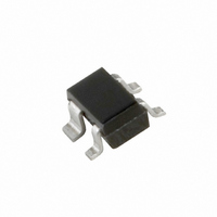
BF1211WR,115 NXP Semiconductors, BF1211WR,115 Datasheet

BF1211WR,115
Specifications of BF1211WR,115
934057513115
BF1211WR
Related parts for BF1211WR,115
BF1211WR,115 Summary of contents
Page 1
DATA SHEET BF1211; BF1211R; BF1211WR N-channel dual-gate MOS-FETs Product specification DISCRETE SEMICONDUCTORS 2003 Dec 16 ...
Page 2
... NXP Semiconductors N-channel dual-gate MOS-FETs FEATURES Short channel transistor with high forward transfer admittance to input capacitance ratio Low noise gain controlled amplifier Excellent low frequency noise performance Partly internal self-biasing circuit to ensure good cross-modulation performance during AGC and good DC stabilization ...
Page 3
... NXP Semiconductors N-channel dual-gate MOS-FETs This product is supplied in anti-static packing to prevent damage caused by electrostatic discharge during transport and handling. ORDERING INFORMATION TYPE NUMBER NAME BF1211 BF1211R BF1211WR LIMITING VALUES In accordance with the Absolute Maximum Rating System (IEC 60134). ...
Page 4
... NXP Semiconductors N-channel dual-gate MOS-FETs 250 handbook, halfpage P tot (mW) 200 (2) 150 100 100 (1) BF1211WR. (2) BF1211; BF1211R. Fig.4 Power derating curve. STATIC CHARACTERISTICS = 25 C unless otherwise specified SYMBOL PARAMETER V drain-source breakdown voltage (BR)DSS V gate 1-source breakdown voltage (BR)G1-SS V gate 2-source breakdown voltage ...
Page 5
... NXP Semiconductors N-channel dual-gate MOS-FETs DYNAMIC CHARACTERISTICS = 25 C; V Common source; T amb SYMBOL PARAMETER y forward transfer admittance fs C input capacitance at gate 1 ig1-ss C input capacitance at gate 2 ig2-ss C output capacitance oss C reverse transfer capacitance MHz rss F noise figure G power gain tr X cross-modulation ...
Page 6
... NXP Semiconductors N-channel dual-gate MOS-FETs 25 handbook, halfpage I D (1) (mA) (2) ( 2.5 V. G2-S G2-S ( 3 G2-S G2 1.5 V. G2-S G2-S Fig.5 Transfer characteristics; typical values. 100 handbook, halfpage I G1 (μ 0 2.5 V. G2-S G2-S ( 3 G2-S G2 1.5 V. G2-S G2-S Fig ...
Page 7
... NXP Semiconductors N-channel dual-gate MOS-FETs 20 handbook, halfpage I D (mA G2 Fig.9 Drain current as a function of gate 1 current; typical values. 20 handbook, halfpage I D (mA connected k. ( k ( k. ( k ( k. ( 100 k Fig.11 Drain current as a function of gate 1 (V and drain supply voltage; typical values. ...
Page 8
... NXP Semiconductors N-channel dual-gate MOS-FETs 50 handbook, halfpage I G1 (μ k (connected ( ( ( 4 Fig.13 Gate 1 current as a function of gate 2 voltage; typical values. 120 handbook, halfpage V unw (dBμV) 110 100 k (connected see Fig.21 MHz MHz; T unw Fig.15 Unwanted voltage for 1% cross-modulation as a function of gain reduction ...
Page 9
... NXP Semiconductors N-channel dual-gate MOS-FETs 2 10 handbook, halfpage y is (mS − mA amb Fig.17 Input admittance as a function of frequency; typical values handbook, halfpage | (mS mA amb Fig.19 Forward transfer admittance and phase as functions of frequency; typical values. 2003 Dec 16 MDB841 handbook, halfpage | (μ (MHz) ...
Page 10
... NXP Semiconductors N-channel dual-gate MOS-FETs handbook, full pagewidth R GEN 50 Ω Table 1 Scattering parameters MAGNITUDE ANGLE (MHz) (ratio) (deg) 3.86 50 0.987 7.73 100 0.985 15.25 200 0.979 22.84 300 0.965 30.15 400 0.949 30.25 500 0.929 44.24 600 0.904 51.16 700 0.876 ...
Page 11
... NXP Semiconductors N-channel dual-gate MOS-FETs PACKAGE OUTLINES Plastic surface-mounted package; 4 leads DIMENSIONS (mm are the original dimensions UNIT max 1.1 0.48 0.88 0.1 mm 0.9 0.38 0.78 OUTLINE VERSION IEC SOT143B 2003 Dec scale 0.15 3.0 1.4 1.9 1.7 0.09 2.8 1.2 REFERENCES ...
Page 12
... NXP Semiconductors N-channel dual-gate MOS-FETs Plastic surface-mounted package; reverse pinning; 4 leads DIMENSIONS (mm are the original dimensions UNIT max 1.1 0.48 0.88 0.1 mm 0.9 0.38 0.78 OUTLINE VERSION IEC SOT143R 2003 Dec scale 0.15 3.0 1.4 1.9 1.7 0.09 2.8 1.2 REFERENCES ...
Page 13
... NXP Semiconductors N-channel dual-gate MOS-FETs Plastic surface-mounted package; reverse pinning; 4 leads DIMENSIONS (mm are the original dimensions UNIT max 1.1 0.4 0.7 mm 0.1 0.8 0.3 0.5 OUTLINE VERSION IEC SOT343R 2003 Dec scale 0.25 2.2 1.35 1.3 1.15 0.10 1.8 1.15 REFERENCES ...
Page 14
... In no event shall NXP Semiconductors be liable for any indirect, incidental, punitive, special or consequential damages (including - without limitation - lost profits, lost savings, business interruption, costs related to the ...
Page 15
... NXP Semiconductors’ specifications such use shall be solely at customer’s own risk, and (c) customer fully indemnifies NXP Semiconductors for any liability, damages or failed product claims resulting from customer design and use of the product for automotive applications beyond NXP Semiconductors’ ...
Page 16
... Interface, Security and Digital Processing expertise Customer notification This data sheet was changed to reflect the new company name NXP Semiconductors, including new legal definitions and disclaimers. No changes were made to the technical content, except for package outline drawings which were updated to the latest version. ...


