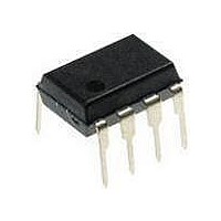
ATTINY12L-4PU Atmel, ATTINY12L-4PU Datasheet - Page 32

ATTINY12L-4PU
Manufacturer Part Number
ATTINY12L-4PU
Description
MCU 8-Bit ATtiny AVR RISC 1KB Flash 3.3V/5V 8-Pin PDIP
Manufacturer
Atmel
Datasheet
1.ATTINY12V-1SI.pdf
(94 pages)
Specifications of ATTINY12L-4PU
Package
8PDIP
Device Core
AVR
Family Name
ATtiny
Maximum Speed
4 MHz
Operating Supply Voltage
3.3|5 V
Data Bus Width
8 Bit
Number Of Programmable I/os
6
Interface Type
SPI
Number Of Timers
1
Program Memory Size
1 KB
Program Memory Type
Flash
Operating Temperature
-40 to 85 °C
Processor Series
ATTINY1x
Core
AVR8
Maximum Clock Frequency
4 MHz
Maximum Operating Temperature
+ 85 C
Mounting Style
Through Hole
Package / Case
PDIP-8
3rd Party Development Tools
EWAVR, EWAVR-BL
Development Tools By Supplier
ATAVRDRAGON, ATSTK500
Minimum Operating Temperature
- 40 C
Lead Free Status / Rohs Status
Details
Pin Change Interrupt
Register Description
MCU Control Register –
MCUCR
32
ATtiny11/12
The pin change interrupt is triggered by any change on any input or I/O pin. Change on
pins PB2..0 will always cause an interrupt. Change on pins PB5..3 will cause an inter-
rupt if the pin is configured as input or I/O, as described in the section “Pin Descriptions”
on page 5. Observe that, if enabled, the interrupt will trigger even if the changing pin is
configured as an output. This feature provides a way of generating a software interrupt.
Also observe that the pin change interrupt will trigger even if the pin activity triggers
another interrupt, for example, the external interrupt. This implies that one external
event might cause several interrupts.
The MCU Control Register contains control bits for general MCU functions.
Note:
• Bit 7 - Res: Reserved Bit
This bit is a reserved bit in the ATtiny11/12 and always reads as zero.
• Bit 6 - Res: Reserved Bit in ATtiny11
This bit is a reserved bit in the ATtiny11 and always reads as zero.
• Bit 6 - PUD: Pull-up Disable in ATtiny12
Setting this bit, disables all pull-ups on port B. If this bit is cleared, the pull-ups can be
individually enabled as described in section “I/O Port B” on page 36.
• Bit 5 - SE: Sleep Enable
The SE bit must be set (one) to make the MCU enter the Sleep Mode when the SLEEP
instruction is executed. To avoid the MCU entering the Sleep Mode unless it is the pro-
grammer’s purpose, it is recommended to set the Sleep Enable SE bit just before the
execution of the SLEEP instruction.
• Bit 4 - SM: Sleep Mode
This bit selects between the two available sleep modes. When SM is cleared (zero), Idle
Mode is selected as Sleep Mode. When SM is set (one), Power-down Mode is selected
as Sleep Mode. For details, refer to the paragraph “Sleep Modes” below.
• Bits 3, 2 - Res: Reserved Bits
These bits are reserved bits in the ATtiny11/12 and always read as zero.
Bit
$35
Read/Write
Initial Value
The values on the pins are sampled before detecting edges. If pin change interrupt
is enabled, pulses that last longer than one CPU clock period will generate an
interrupt. Shorter pulses are not guaranteed to generate an interrupt.
The Pull-up Disable (PUD) bit is only available in ATtiny12.
R
7
0
-
(PUD)
R(/W)
6
0
R/W
SE
5
0
R/W
SM
4
0
R
3
0
-
R
2
0
-
ISC01
R/W
1
0
ISC00
R/W
0
0
1006F–AVR–06/07
MCUCR


