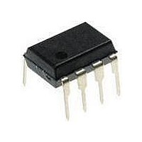
ATTINY12L-4PU Atmel, ATTINY12L-4PU Datasheet - Page 7

ATTINY12L-4PU
Manufacturer Part Number
ATTINY12L-4PU
Description
MCU 8-Bit ATtiny AVR RISC 1KB Flash 3.3V/5V 8-Pin PDIP
Manufacturer
Atmel
Datasheet
1.ATTINY12V-1SI.pdf
(94 pages)
Specifications of ATTINY12L-4PU
Package
8PDIP
Device Core
AVR
Family Name
ATtiny
Maximum Speed
4 MHz
Operating Supply Voltage
3.3|5 V
Data Bus Width
8 Bit
Number Of Programmable I/os
6
Interface Type
SPI
Number Of Timers
1
Program Memory Size
1 KB
Program Memory Type
Flash
Operating Temperature
-40 to 85 °C
Processor Series
ATTINY1x
Core
AVR8
Maximum Clock Frequency
4 MHz
Maximum Operating Temperature
+ 85 C
Mounting Style
Through Hole
Package / Case
PDIP-8
3rd Party Development Tools
EWAVR, EWAVR-BL
Development Tools By Supplier
ATAVRDRAGON, ATSTK500
Minimum Operating Temperature
- 40 C
Lead Free Status / Rohs Status
Details
ALU – Arithmetic Logic
Unit
Subroutine and Interrupt
Hardware Stack
1006F–AVR–06/07
Figure 3. The ATtiny11/12 AVR RISC Architecture
A flexible interrupt module has its control registers in the I/O space with an additional
global interrupt enable bit in the status register. All the different interrupts have a sepa-
r a t e i n t e r r u p t v e c t o r i n t h e i n t e r r u p t v e c t o r t a b le a t t h e b e g i n n i n g o f t h e
program memory. The different interrupts have priority in accordance with their interrupt
vector position. The lower the interrupt vector address, the higher the priority.
The high-performance AVR ALU operates in direct connection with all the 32 general-
purpose working registers. Within a single clock cycle, ALU operations between regis-
ters in the register file are executed. The ALU operations are divided into three main
categories – arithmetic, logic and bit-functions. Some microcontrollers in the AVR prod-
uct family feature a hardware multiplier in the arithmetic part of the ALU.
The ATtiny11/12 uses a 3-level-deep hardware stack for subroutines and interrupts. The
hardware stack is 9 bits wide and stores the program counter (PC) return address while
subroutines and interrupts are executed.
RCALL instructions and interrupts push the PC return address onto stack level 0, and
the data in the other stack levels 1-2 are pushed one level deeper in the stack. When a
RET or RETI instruction is executed the returning PC is fetched from stack level 0, and
the data in the other stack levels 1-2 are popped one level in the stack.
If more than three subsequent subroutine calls or interrupts are executed, the first val-
ues written to the stack are overwritten. Pushing four return addresses A1, A2, A3, and
A4, followed by four subroutine or interrupt returns, will pop A4, A3, A2, and once more
A2 from the hardware stack.
Control Lines
Instruction
Instruction
512 x 16
Program
Register
Decoder
Flash
Direct Addressing
8-bit Data Bus
Program
Counter
64 x 8 EEPROM
(ATtiny12 only)
Registers
and Test
General-
purpose
Status
32 x 8
ALU
ATtiny11/12
(ATtiny12 only)
Timer/Counter
Comparator
Registers
Watchdog
Interrupt
I/O Lines
SPI Unit
Control
Analog
Timer
8-bit
Unit
6
7


