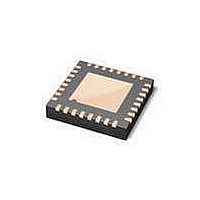
ISP1504CBS NXP Semiconductors, ISP1504CBS Datasheet - Page 11

ISP1504CBS
Manufacturer Part Number
ISP1504CBS
Description
RF Transceiver USB2.0 ULPI OTG TRANSCEIVER
Manufacturer
NXP Semiconductors
Datasheet
1.ISP1504ABS118.pdf
(83 pages)
Specifications of ISP1504CBS
Operating Supply Voltage
1.65 V to 3.6 V
Mounting Style
SMD/SMT
Package / Case
HVQFN
Minimum Operating Temperature
- 40 C
Lead Free Status / RoHS Status
Lead free / RoHS Compliant
Other names
ISP1504CBS,157
Available stocks
Company
Part Number
Manufacturer
Quantity
Price
Part Number:
ISP1504CBS
Manufacturer:
NXP/恩智浦
Quantity:
20 000
Company:
Part Number:
ISP1504CBSFA
Manufacturer:
NXP
Quantity:
6 041
NXP Semiconductors
ISP1504A_ISP1504C_3
Product data sheet
7.6.4 Charge pump
7.9.1 DATA[7:0]
7.7 Band gap reference voltage
7.8 Power-On Reset (POR)
7.9 Detailed description of pins
The ISP1504 uses a built-in charge pump to supply current to V
of 5 V. The charge pump works as a capacitive DC-DC converter. An external holding
capacitor, C
which also shows a typical OTG V
amount of current drive required. If the internal charge pump is not used, the C
capacitor is not required.
For details on the C_A and C_B pins, see
The band gap circuit provides a stable internal voltage reference to bias the analog
circuitry. The band gap requires an accurate external reference resistor R
between the RREF and GND pins. For details, see
The ISP1504 has an internal power-on reset circuit that resets all internal logic on
power-up. The ULPI interface is also reset on power-up.
Remark: When CLOCK starts toggling after power-up, the USB link must issue a reset
command over the ULPI bus to ensure correct operation of the ISP1504.
The ISP1504 is a Physical layer (PHY) containing a USB transceiver. DATA[7:0] is the
bidirectional data bus. The USB link must drive DATA[7:0] to LOW when the ULPI bus is
idle. When the link has data to transmit to the PHY, it drives a nonzero value.
The data bus can be reconfigured to carry various data types, as given in
Section
The DATA[7:0] pins can be 3-stated by driving pin CHIP_SELECT_N to HIGH. Weak
pull-down resistors are incorporated into the DATA[7:0] pins as part of the interface protect
feature. For details, see
Fig 3.
9.
External capacitors connection
cp(C_A)-(C_B)
, is required between the C_A and C_B pins as shown in
Rev. 03 — 7 April 2008
Section
ISP1504
V
9.3.1.
C_B
C_A
BUS
BUS
load. The value of C
Section
0.1 F
C cp(C_A)-(C_B)
ISP1504A; ISP1504C
7.9.8.
Section
4.7 F
OTG V
004aaa515
ULPI HS USB OTG transceiver
cp(C_A)-(C_B)
16.
BUS
BUS
at a nominal voltage
depends on the
© NXP B.V. 2008. All rights reserved.
RREF
Section 8
cp(C_A)-(C_B)
connected
Figure
10 of 82
and
3,


