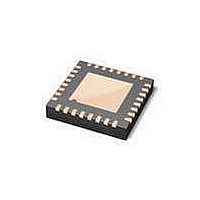
ISP1504CBS NXP Semiconductors, ISP1504CBS Datasheet - Page 7

ISP1504CBS
Manufacturer Part Number
ISP1504CBS
Description
RF Transceiver USB2.0 ULPI OTG TRANSCEIVER
Manufacturer
NXP Semiconductors
Datasheet
1.ISP1504ABS118.pdf
(83 pages)
Specifications of ISP1504CBS
Operating Supply Voltage
1.65 V to 3.6 V
Mounting Style
SMD/SMT
Package / Case
HVQFN
Minimum Operating Temperature
- 40 C
Lead Free Status / RoHS Status
Lead free / RoHS Compliant
Other names
ISP1504CBS,157
Available stocks
Company
Part Number
Manufacturer
Quantity
Price
Part Number:
ISP1504CBS
Manufacturer:
NXP/恩智浦
Quantity:
20 000
Company:
Part Number:
ISP1504CBSFA
Manufacturer:
NXP
Quantity:
6 041
NXP Semiconductors
Table 2.
[1]
[2]
[3]
[4]
ISP1504A_ISP1504C_3
Product data sheet
Symbol
V
REG3V3
XTAL1
XTAL2
RESET_N
REG1V8
DIR
STP
NXT
V
DATA7
DATA6
DATA5
DATA4
CLOCK
DATA3
CHIP_SELECT_N
V
DATA2
DATA1
GND
BUS
CC(I/O)
CC(I/O)
Symbol names ending with an underscore N, for example, NAME_N, indicate active LOW signals.
For details on external components required on each pin, see bill of materials and application diagrams in
I = input; O = output; I/O = digital input/output; OD = open-drain output; AI = analog input; AO = analog output; AI/O = analog
input/output; P = power or ground pin.
A detailed description of these pins can be found in
[1][2]
Pin description
Pin
13
14
15
16
17
18
19
20
21
22
23
24
25
26
27
28
29
30
31
32
die
pad
…continued
Type
AI/O
P
AI
AO
I
P
O
I
O
P
I/O
I/O
I/O
I/O
O
I/O
I
P
I/O
I/O
P
[3]
Description
V
5 V tolerant
3.3 V regulator output
crystal oscillator or clock input
crystal oscillator output
active LOW, asynchronous reset input
plain input
1.8 V regulator output
ULPI direction signal
slew-rate controlled output (1 ns)
ULPI stop signal
plain input; programmable pull up
ULPI next signal
slew-rate controlled output (1 ns)
I/O supply rail
pin 7 of the bidirectional ULPI data bus
slew-rate controlled output (1 ns); plain input; programmable pull down
pin 6 of the bidirectional ULPI data bus
slew-rate controlled output (1 ns); plain input; programmable pull down
pin 5 of the bidirectional ULPI data bus
slew-rate controlled output (1 ns); plain input; programmable pull down
pin 4 of the bidirectional ULPI data bus
slew-rate controlled output (1 ns); plain input; programmable pull down
60 MHz clock output
slew-rate controlled output (1 ns)
pin 3 of the bidirectional ULPI data bus
slew-rate controlled output (1 ns); plain input; programmable pull down
active LOW chip select
plain input
I/O supply rail
pin 2 of the bidirectional ULPI data bus
slew-rate controlled output (1 ns); plain input; programmable pull down
pin 1 of the bidirectional ULPI data bus
slew-rate controlled output (1 ns); plain input; programmable pull down
ground supply; down bonded to the exposed die pad (heat sink); to be connected to
the PCB ground
BUS
pin of the USB cable
Section
Rev. 03 — 7 April 2008
[4]
7.9.
ISP1504A; ISP1504C
ULPI HS USB OTG transceiver
Section
© NXP B.V. 2008. All rights reserved.
16.
6 of 82


